Piezoelectric/electrostrictive film type device and method of manufacturing the same

a film type, electroelectric technology, applied in the direction of device material selection, basic electric elements, generators/motors, etc., can solve the problems of unavoidable lead in the pzt-based composition, easy to be regarded, and difficult to obtain large displacement, etc., to achieve superior piezoelectric/electrostrictive characteristics, large displacement, and high consideration of environments

Inactive Publication Date: 2006-03-30
NGK INSULATORS LTD
View PDF14 Cites 22 Cited by
  • Summary
  • Abstract
  • Description
  • Claims
  • Application Information

AI Technical Summary

Benefits of technology

[0053] According to the first and second piezoelectric/electrostrictive film type devices of the present invention, lead (Pb) is not contained, and considerations are highly given to environments. The first and second piezoelectric/electrostrictive film type devices of the present invention produce an effect that a displacement generated in the piezoelectric/electrostrictive operating portion is remarkably effectively transmitted to the substrate, a superior piezoelectric/electrostrictive ch

Problems solved by technology

Additionally, the PZT-based composition unavoidably contains lead (Pb).
Especially, in recent years, an influence on global environments, such as elution of lead (Pb) due to acid rain, has tended to be regarded as a problem.
However, as to the piezoelectric article or the

Method used


Image

  • Piezoelectric/electrostrictive film type device and method of manufacturing the same
  • Piezoelectric/electrostrictive film type device and method of manufacturing the same
  • Piezoelectric/electrostrictive film type device and method of manufacturing the same

Examples


examples

[0116] The present invention will be specifically described hereinafter based on examples, but the present invention is not limited to these examples. There will be described methods of measuring various physical values, and methods of evaluating characteristics.

[0117] [Flexural Displacement]: A flexural displacement (μm) generated when applying a voltage between upper and lower electrode films in such a manner as to obtain an electric field of 3 kV / mm was measured with a laser displacement measurement unit. It is to be noted that in tables, an “average” of the “flexural displacement (μm)” is an average value in a case where ten piezoelectric / electrostrictive film type devices were manufactured in each of an example and a comparative example, and the flexural displacements of the devices were measured. A “fluctuation” refers to a difference between a maximum value and a minimum value of the measured flexural displacement.

[0118] [Concentration of Various Types of Oxides contained i...

examples 1 to 8

, Comparative Examples 1, 2

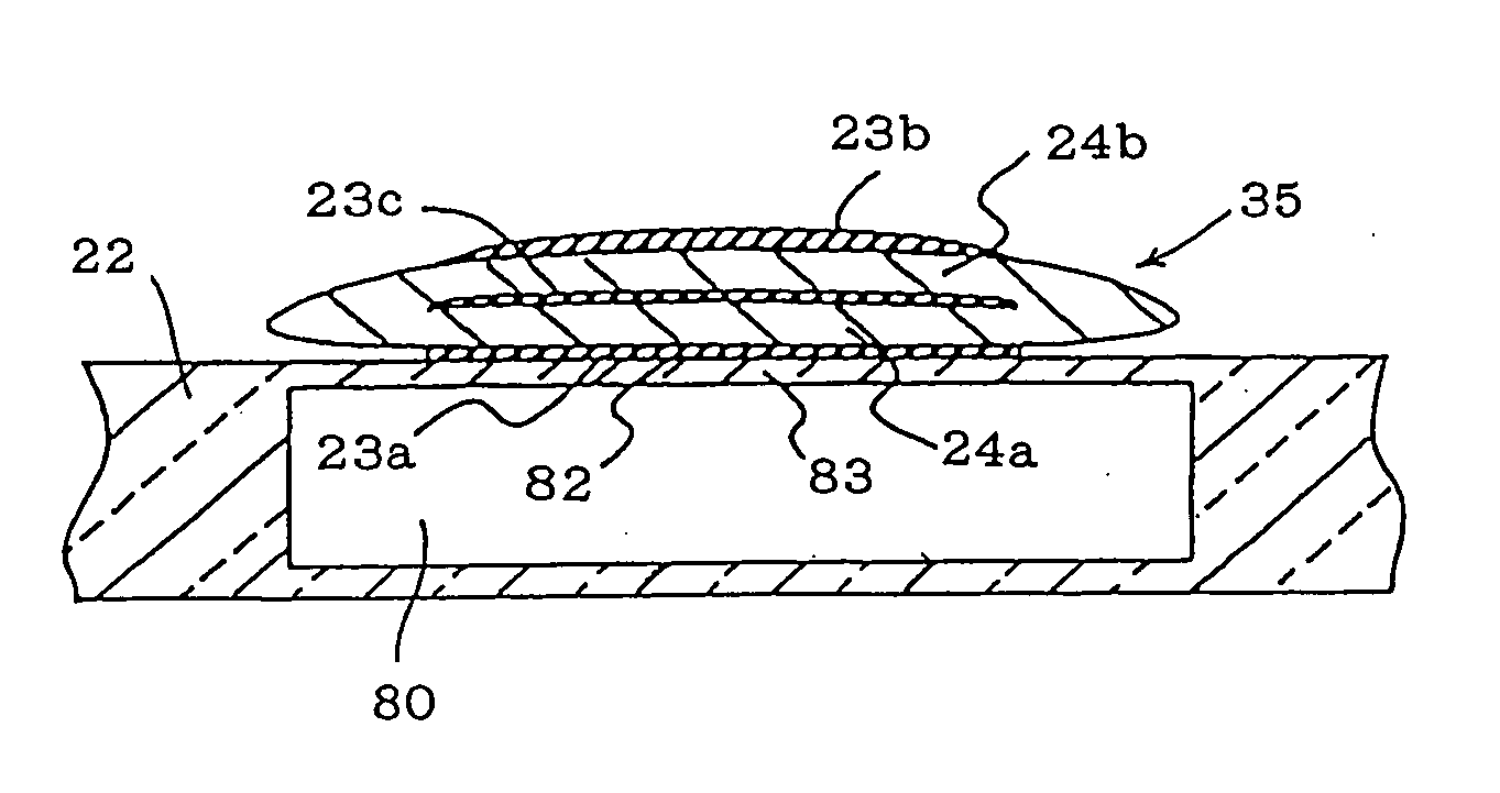
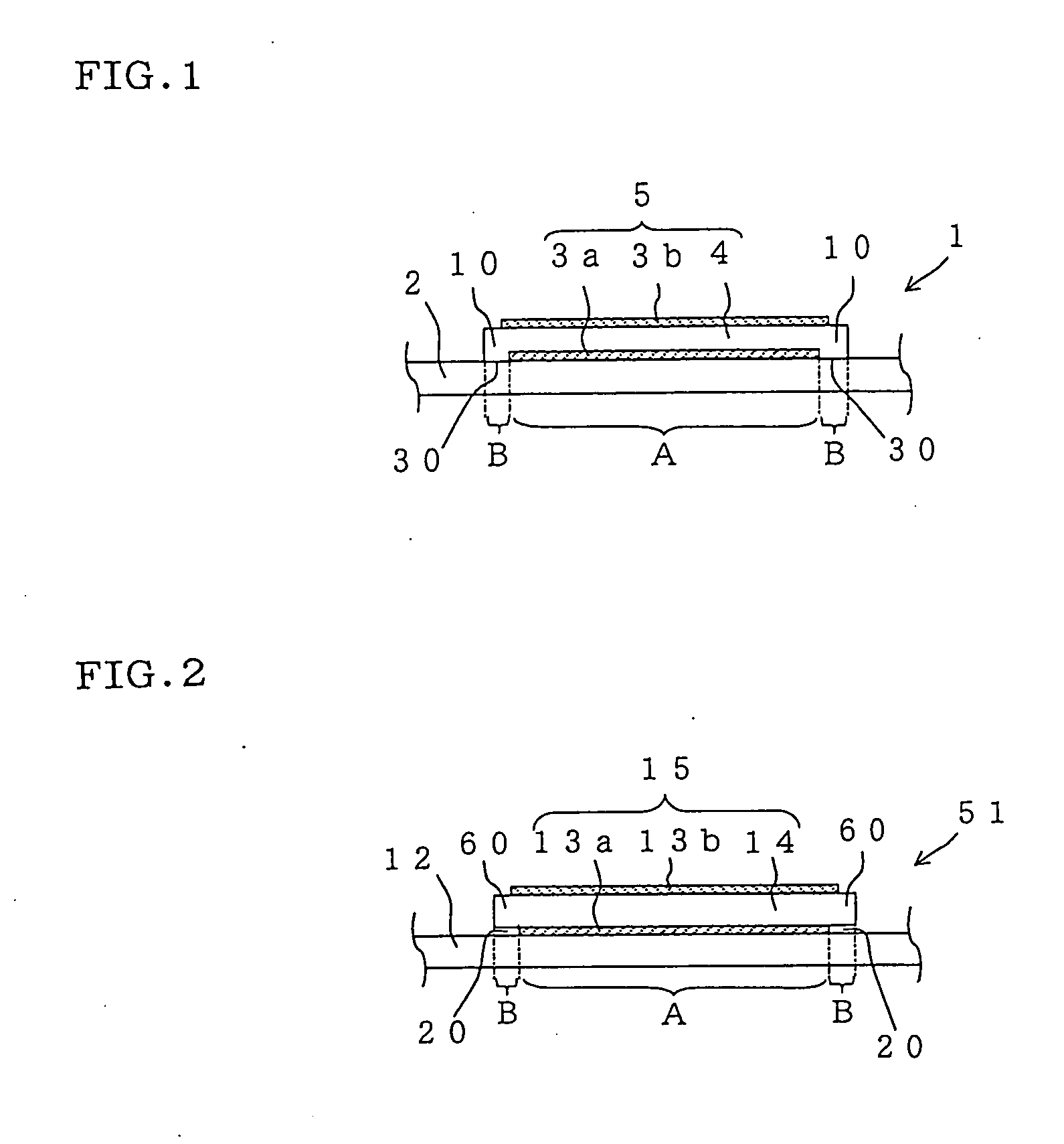
[0122] On a substrate (1.6×1.1 mm×thickness of 100 μm) made of zirconia (ZrO2) formed by a green sheet laminating process, fired, and stabilized by yttria (Y2O3), a lower electrode film (1.2×0.8 mm×thickness of 3 μm) made of platinum (Pt) was formed by a screen printing process, and formed integrally with the substrate by a thermal treatment at 1300° C. for two hours. On the lower electrode film, each piezoelectric / electrostrictive composition represented by a predetermined composition formula was laminated with a dimension 1.3×0.9 mm×thickness of 15 μm by the screen printing process. It is to be noted that the piezoelectric / electrostrictive composition was laminated by performing the printing twice to prepare: (1) a composition in which an organic matter content of a first layer was set to be larger by 10 mass % than that of a second layer (detached state); and (2) a composition in which the organic matter content of the first layer was set to be equal to...

example 9

[0124] On a substrate (1.6×1.1 mm×thickness of 100 μm) made of zirconia (ZrO2) formed by a green sheet laminating process, fired, and stabilized by yttria (Y2O3), a lower electrode film (1.2×0.8 mm×thickness of 3 μm) made of platinum (Pt) was formed by a screen printing process, and formed integrally with the substrate by a thermal treatment at 1300° C. for two hours. A piezoelectric / electrostrictive composition material was obtained using a material compound containing potassium (K), sodium (Na), niobium (Nb), and tantalum (Ta), respectively, more by 3 mass % in terms of the element as compared with a theoretical necessary amount calculated from a general formula “(Li0.06K0.45Na0.49)0.991 (Nb0.92Ta0.08)O3”. On the lower electrode film, the material was laminated with a dimension 1.3×0.9 mm×thickness of 15 μm by the screen printing process, and fired at 1000° C. for three hours. Furthermore, on the composition, an upper electrode film (1.2×0.8 mm×thickness of 0.5 μm) made of gold (A...


PUM

PropertyMeasurementUnit
Lengthaaaaaaaaaa
Fractionaaaaaaaaaa
Fractionaaaaaaaaaa

Abstract

There is disclosed a piezoelectric/electrostrictive film type device 1 provided with: a thin substrate 2 made of a ceramic; and a piezoelectric/electrostrictive operating portion 5 disposed on the substrate 2 and constituted by successively laminating a lower electrode film 3a, a piezoelectric/electrostrictive film 4 containing a large number of crystal particles constituted of a piezoelectric/electrostrictive composition, and an upper electrode film 3b. The piezoelectric/electrostrictive composition contains one or more alkali metal elements selected from the group consisting of lithium (Li), potassium (K), and sodium (Na), and one or more metal elements selected from the group consisting of niobium (Nb), tantalum (Ta), antimony (Sb), and silver (Ag) (however, surely containing niobium (Nb), and circle equivalent diameters of 90% or more of the large number of crystal particles are in a range of 0.3 to 50 μm. It is possible to exhibit a superior piezoelectric/electrostrictive characteristic without containing lead (Pb) and obtain an especially large displacement.

Description

BACKGROUND OF THE INVENTION [0001] 1. Field of the Invention [0002] The present invention relates to a piezoelectric / electrostrictive film type device, and a method of manufacturing the device, more particularly to a piezoelectric / electrostrictive film type device which exhibits superior piezoelectric / electrostrictive characteristics and in which considerations are given to even environments, and a method of manufacturing the device. [0003] 2. Description of the Related Art [0004] Heretofore, a piezoelectric / electrostrictive device has been known as a device capable of controlling micro displacement of the order of sub-microns. Especially, a piezoelectric / electrostrictive film type device is preferable for the control of the micro displacement. In the film type device, a piezoelectric / electrostrictive portion constituted of a piezoelectric / electrostrictive composition and an electrode portion to which a voltage is applied are laminated on a substrate made of a ceramic. Additionally,...

Claims


Application Information

Patent Timeline
IPC IPC(8): H01L41/18
CPCC04B35/495C04B2235/3201C04B2235/3203C04B2235/3251C04B2235/3291C04B2235/3294Y10T29/42C04B2235/6567C04B2235/785C04B2235/786H01L41/0973H01L41/1873H01L41/314C04B2235/656H10N30/2047H10N30/8542H10N30/074
Inventor NANATAKI, TSUTOMUYAMAGUCHI, HIROFUMIKASHIWAYA, TOSHIKATSUKOIZUMI, TAKAAKI
Owner NGK INSULATORS LTD
Why Eureka
Try Eureka