
Low power consumption magnetic memory and magnetic information recording device

a magnetic memory and low power consumption technology, applied in semiconductor devices, digital storage, instruments, etc., can solve the problem of not being able to drastically reduce the current which was necessary, and achieve the effect of reducing the threshold current, high output magnetic memory, and decreasing the demagnetizing field

Active Publication Date: 2006-03-30
TOHOKU UNIV
View PDF3 Cites 27 Cited by
  • Summary
  • Abstract
  • Description
  • Claims
  • Application Information

AI Technical Summary

Benefits of technology

"The present invention provides a low power consumption magnetic memory cell that reduces the current required for spin transfer torque magnetization reversal. This is achieved by separately forming a stacked film of a ferromagnetic layer, a non-magnetic layer, and a ferromagnetic layer in a film surface and reducing the demagnetizing field of the recording magnetic layer. The magnetic memory uses a writing method using a spin torque magnetization in the film surface which does not use a magnetic field induced by a current and a reading method using a TMR element, resulting in a high output magnetic memory with extremely low power consumption."

Problems solved by technology

The ferromagnetic layer which performs magnetization reversal was a thin film and the influence of the demagnetizing field in the direction perpendicular to the film surface was great, so that a problem arose in that it was impossible to drastically reduce the current which was necessary to perform the magnetization reversal.

Method used


Image

  • Low power consumption magnetic memory and magnetic information recording device
  • Low power consumption magnetic memory and magnetic information recording device
  • Low power consumption magnetic memory and magnetic information recording device

Examples


first embodiment

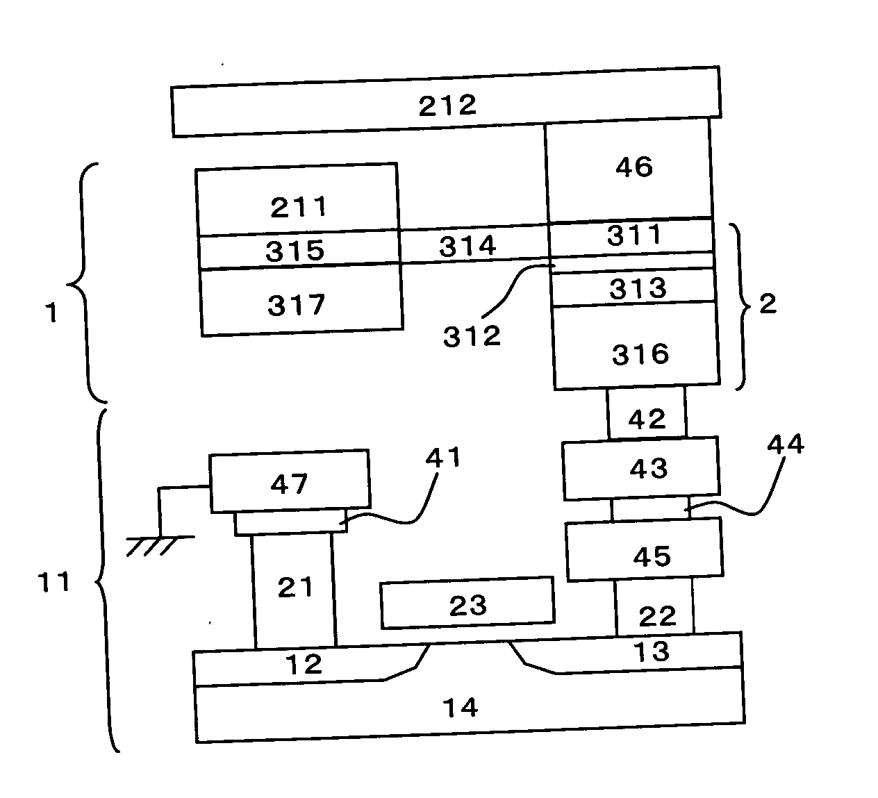
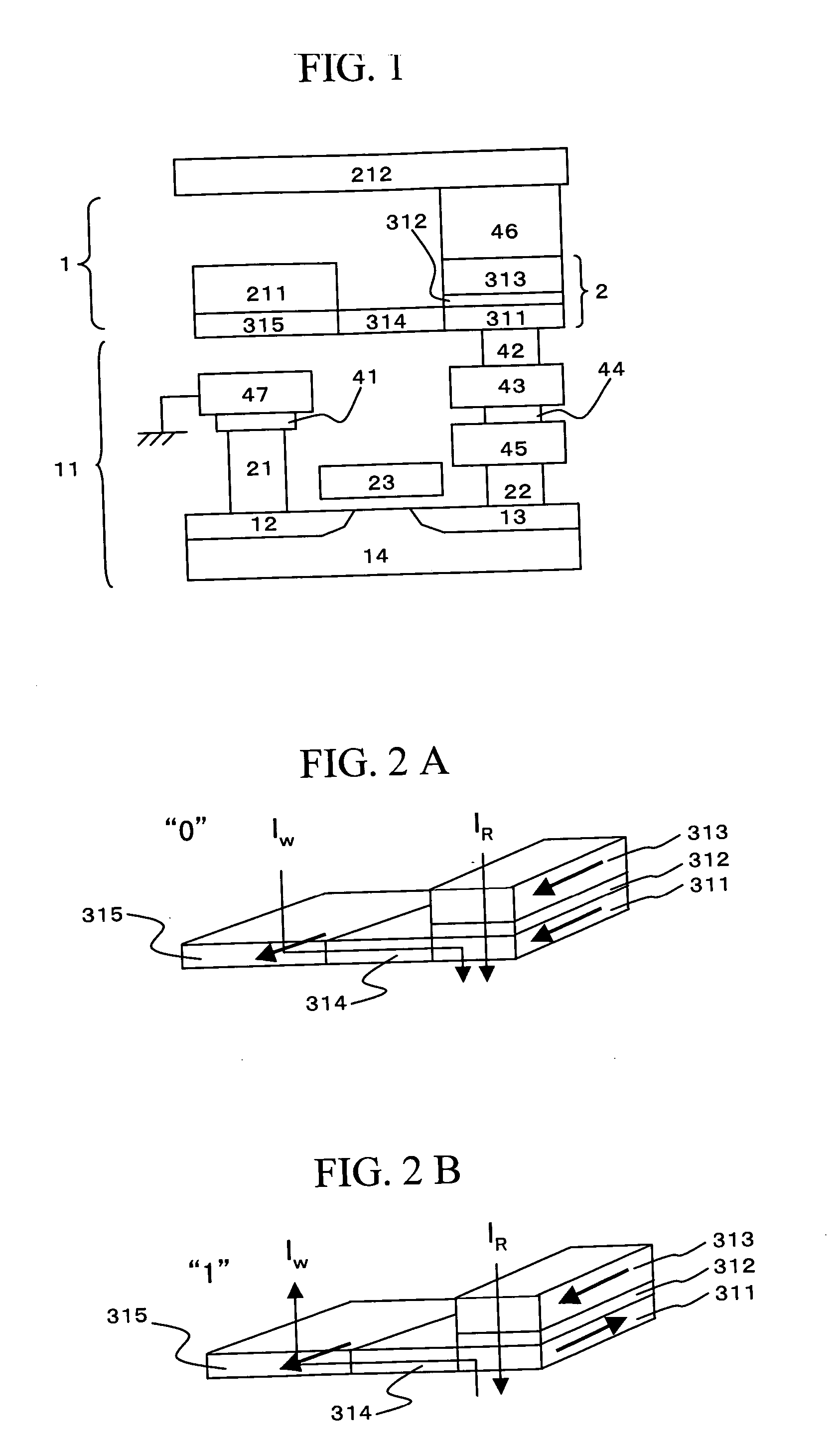
[0023]FIG. 1 is a cross-sectional schematic drawing illustrating an example of a configuration of a magnetic memory and a switching portion of a memory cell. A C-MOS transistor 11 consists of two n-type semiconductors 12 and 13 and a p-type semiconductor 14. The electrode 21 to be a drain is electrically connected to the n-type semiconductor 12 and connected to the ground through the electrode 41 and the electrode 47. The electrode 22 to be a source is connected to the n-type semiconductor 13. Moreover, 23 is a gate electrode, and on / off operation of the current flowing between the source electrode 22 and the drain electrode 21 is controlled by on / off operation of this gate electrode 23. The electrode 45, electrode 44, electrode 43, and electrode 42 are stacked on the source electrode 22, and the free layer 311 is connected to the electrode 42. The tunneling magnetoresistive element (TMR element) of the memory cell 1 consists of a stacked layer of the free layer 311, the insulation ...

second embodiment

[0030]FIG. 6 is a cross-sectional schematic drawing illustrating another example of a memory cell and a switching portion of a magnetic memory of the present invention. This embodiment corresponds to one in which the first anti-ferromagnetic layer 316 and the second anti-ferromagnetic layer 317 are stacked to fix the magnetization directions of the first pinned layer 313 and the second pinned layer 315, respectively, in one direction in the configuration of the memory cell 1 shown in FIG. 1.

[0031] In this embodiment, PtMn (12 nm) was used for the first anti-ferromagnetic layer 316 and the second anti-ferromagnetic layer 317. Herein, except for PtMn, FeMn and IrMn may be used for the anti-ferromagnetic layer. In this embodiment, since the magnetic domains of the pinned layer are controlled to be oriented in one direction due to the anti-ferromagnetic layer, parallel and anti-parallel states of the relative angle of the magnetization direction with the free layer can be achieved stab...

third embodiment

[0033]FIG. 8 is a cross-sectional schematic drawing illustrating another example of a memory cell and a switching portion of a magnetic memory of the present invention. This embodiment shows an example of the configuration, in which the first pinned layer 313 is formed on the transistor 11 side through the insulation barrier layer 312, in the configuration of the memory cell 1 shown in FIG. 1. A magnetic memory of this embodiment can be deposited without breaking the vacuum atmosphere in a manufacturing process of the magnetic memory portion and a high quality TMR element can be fabricated, so that the output of the read signal can be increased.

[0034]FIG. 9 shows an example illustrating a method of reading / writing magnetic information to the free layer 311. The method of reading / writing magnetic information is same as that of the first embodiment. When the magnetization direction of the free layer 311 of the TMR element 2 is made parallel to the magnetization direction of the first...


PUM


Abstract

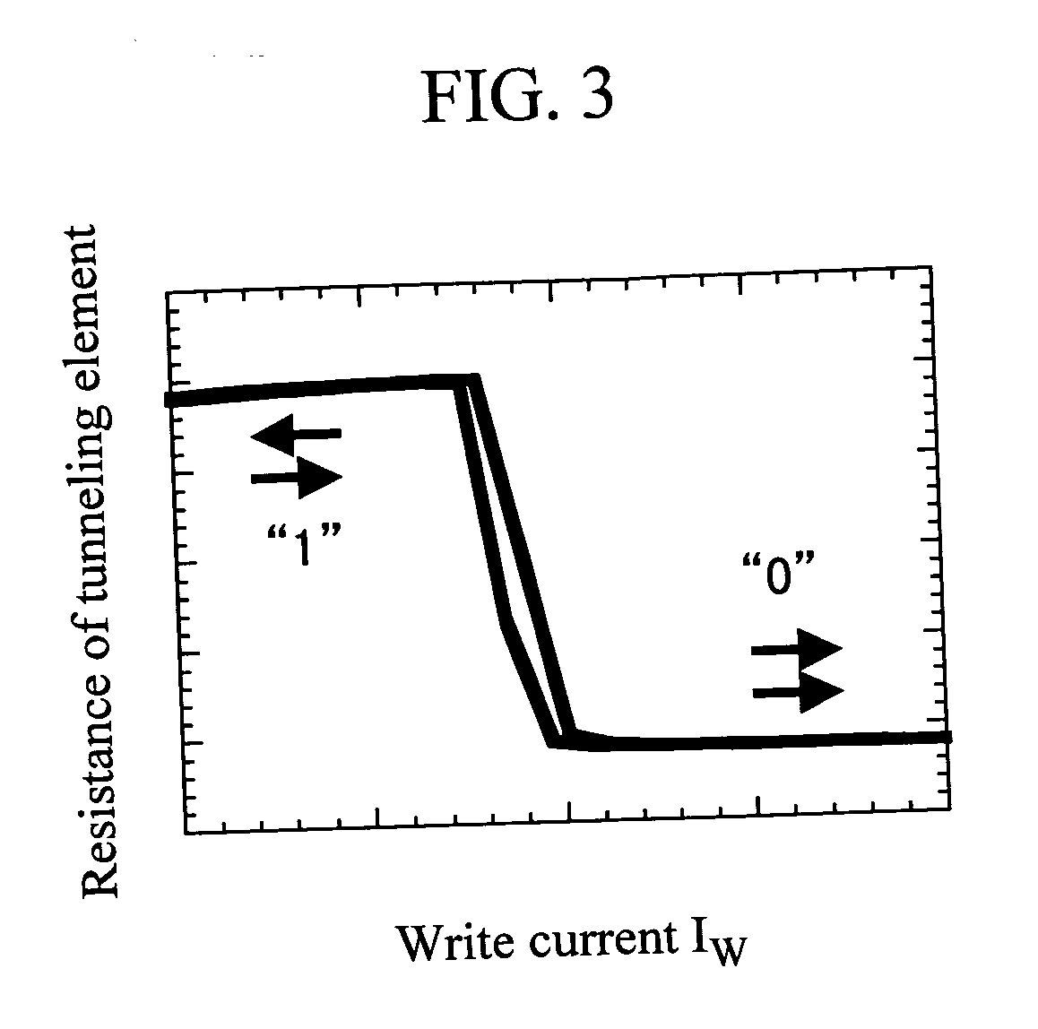
A highly integrated magnetic memory with low power consumption is provided. A first element portion which has a free layer, a first pinned layer formed in the film thickness direction of the free layer, and an insulation barrier layer formed between the free layer and the first pinned layer, and a second element portion which has the aforementioned free layer, a second pinned layer formed in the film surface direction of the free layer, and a non-magnetic layer formed between the free layer and the second pinned layer are provided. A current IW flows in the film surface direction of the second element portion for writing the magnetic information and a current IR flows in the film thickness direction of the first element portion for reading the magnetic information.

Description

CLAIM OF PRIORITY [0001] The present application claims priority from Japanese application JP 2004-279648 filed on Sep. 27, 2004, the content of which is hereby incorporated by reference into this application. FIELD OF THE INVENTION [0002] The present invention relates to a low power consumption and high output magnetic memory and magnetic information recording device which has both a switching function and a spin torque magnetization reversal function. BACKGROUND OF THE INVENTION [0003] A magnetic memory of the prior art consists of a memory cell 1 in which a tunneling magnetoresistive element (TMR element) is formed on a MOSFET, as shown in FIG. 13. The TMR element of the memory cell 1 ((T. Miyazaki and N. Tezuka, J. Magn. Magn. Mater. 139, L231 (1995)) consists of a free layer 31, an insulation barrier layer 32, and a pinned layer 33, and is connected to a bit line 212 and an electrode circuit 46. The electrode circuit 46 is connected to the source electrode 22 of MOSFETs 12 to 1...

Claims


Application Information

Patent Timeline
Patent Type & Authority Applications(United States)
IPC IPC(8): G11C11/14
CPCG11C11/16
Inventor HAYAKAWA, JUNOHNO, HIDEO
Owner TOHOKU UNIV
Learn More