

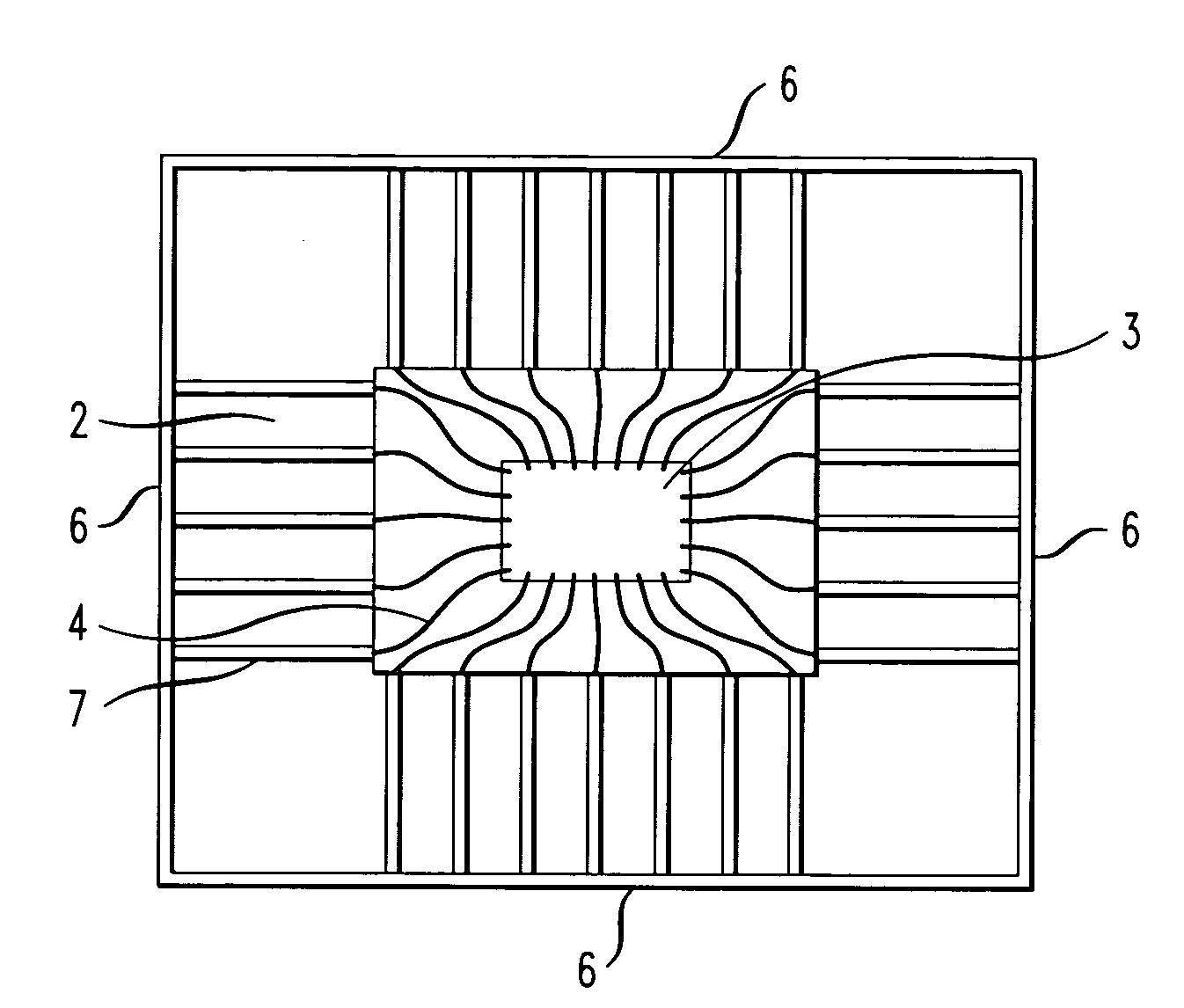
Whisker-free lead frames
a lead frame and whisker technology, applied in the field of tin containing interconnects, can solve problems such as the potential to produce mechanical instabilities, and achieve the effect of reducing the proclivity to induce mechanical instabilities
- Summary
- Abstract
- Description
- Claims
- Application Information
AI Technical Summary
Benefits of technology
Problems solved by technology
Method used
Image

Examples
example
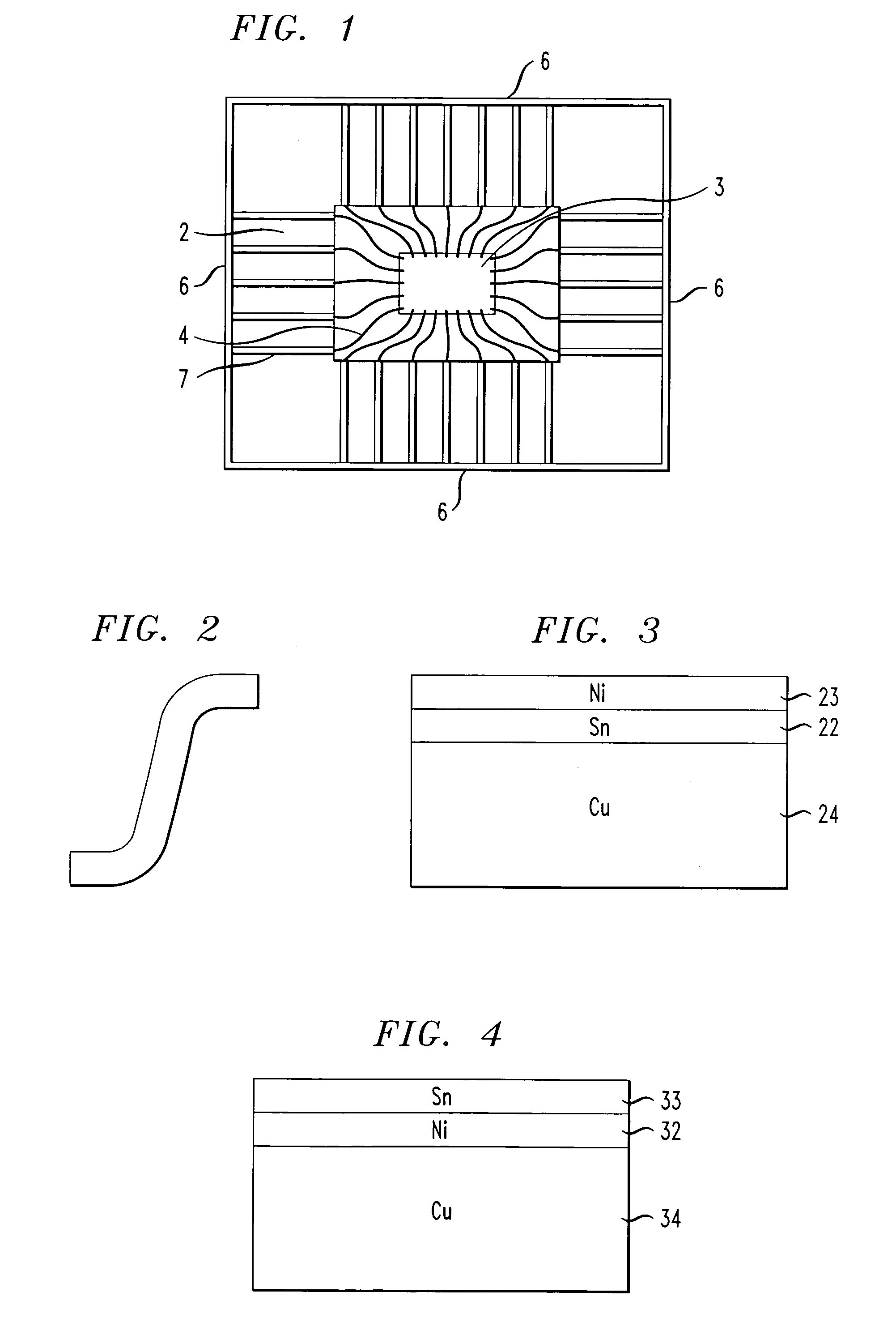
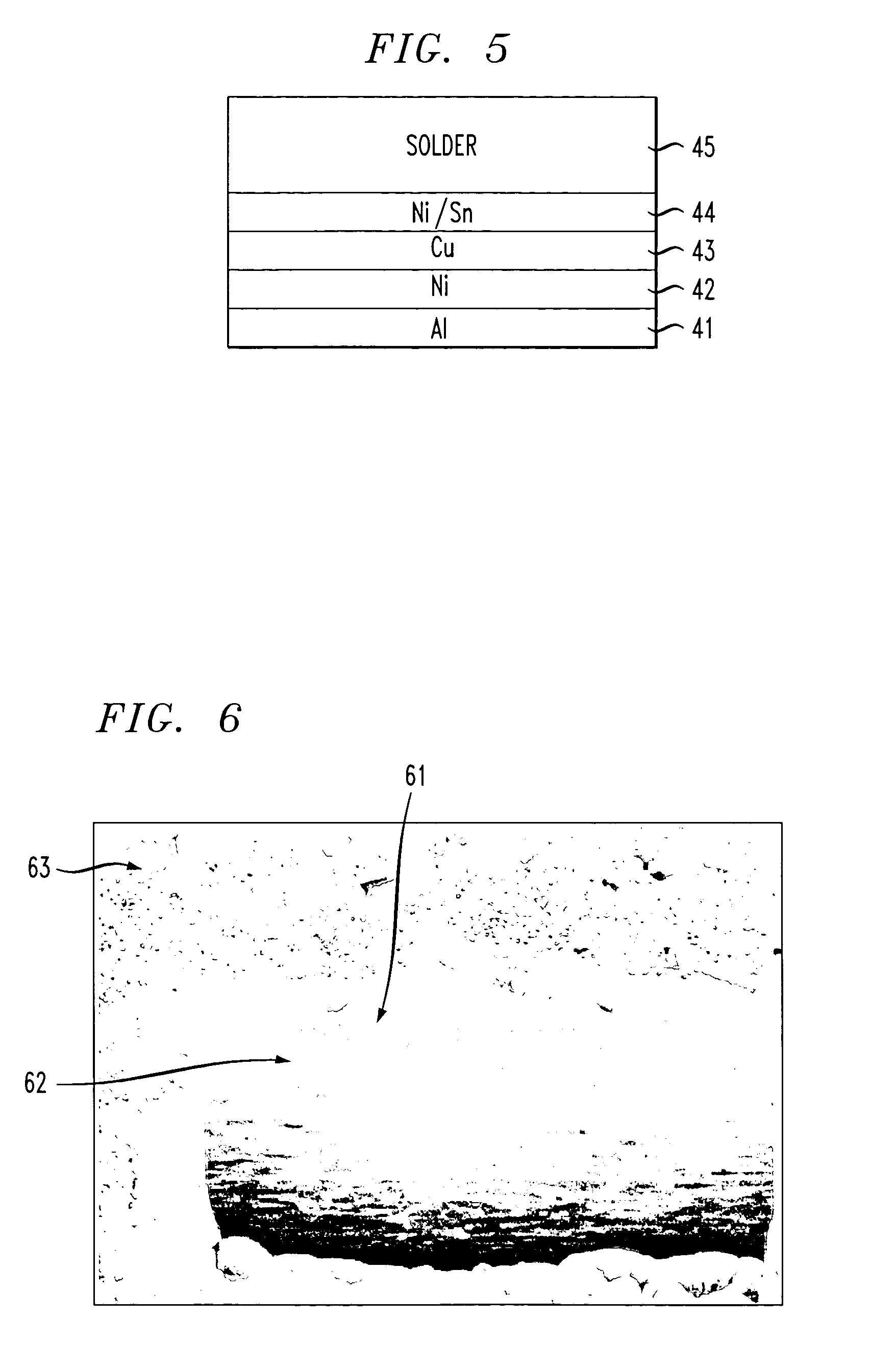
[0019] A 0.25 um thick nickel layer was electroplated onto a copper lead frame. Subsequently a 3 um thick tin layer was electroplated onto the nickel layer. On a weight percentage basis the sample contains approximately 4% nickel and 96% tin. The device was then subjected to a 150° C. 1 hour anneal. Finally the device was subjected to a typical solder reflow process with a peak temperature of 260° C. The time the device was at 260° C. was approximately 18 seconds. A secondary electron image was taken from a focused ion beam cross section of the sample. As shown in FIG. 6, the entire tin layer is converted into a planar nickel / copper / tin intermetallic layer 61 on the copper lead 62. The platinum layer 63 was deposited onto the sample prior to focused ion beam cutting and acts as a reference that defines the surface of the tin / Ni / Cu layer.
PUM
| Property | Measurement | Unit |
|---|---|---|
| Temperature | aaaaa | aaaaa |
| Temperature | aaaaa | aaaaa |
| Fraction | aaaaa | aaaaa |
Abstract
Description
Claims
Application Information