Method for fabricating carrier structure integrated with semiconductor element

a carrier structure and semiconductor technology, applied in the field of carrier structure integration of semiconductor elements, can solve the problems of complex fabrication process, increased overall height of the package, and inability to facilitate size miniaturization, so as to simplify the overall fabrication process and reduce the fabrication cost

Inactive Publication Date: 2006-03-30
PHOENIX PRECISION TECH CORP
View PDF1 Cites 19 Cited by
  • Summary
  • Abstract
  • Description
  • Claims
  • Application Information

AI Technical Summary

Benefits of technology

[0015] The semiconductor element is fixed in the opening of the carrier by the means of the first photosensitive insulating layer. The first photosensitive insulating layer is patterned to form the recessed grooves such as contact holes and circuit slots. Then, the build-up circuit such as a conductive bump and a circuit layer is formed in the recessed grooves respectively. Therefore, the procedure of fixing the semiconductor element in the carrier and the procedure of fabricating the build-up circuit are combined in the same set of fabrication processes for the carrier structure, thereby effectively simplifying the overall fabrication processes and reducing the fabrication cost.

Problems solved by technology

Such stacking arrangement increases the overall height of the package and does not facilitate size miniaturization thereof.
Moreover, for either of the flip-chip package or wire-bonded package, fabrication of the packaging substrate and encapsulation of the semiconductor chip employ different fabrication apparatuses and processes, which involve complex fabrication processes and require high fabrication cost.
However, since practically the mold is restricted by the design of the semiconductor package, and the size of mold cavity and clamping positions of the mold may not be precisely made, the substrate cannot be strongly clamped by the mold, and the injected resin material would easily flash to unintended areas on the substrate.
This not only degrades the surface planarity and appearance of the semiconductor package, but also may contaminate predetermined positions on the substrate for subsequently mounting solder balls.
As a result, the quality of electrical connection of the semiconductor package is adversely affected, and the yield and reliability of the semiconductor package are also deteriorated.
Therefore, different manufacturers (including carrier manufacturer and package manufacturer) are involved in the fabrication of semiconductor packages, and the practical fabrication processes are complicated and difficult in interface integration.
Moreover, if the functional design of packages is to be altered, the associated changes and interface integration would become more complex and difficult, thereby not providing sufficient flexibility in design alternation and economical benefits.

Method used


Image

  • Method for fabricating carrier structure integrated with semiconductor element
  • Method for fabricating carrier structure integrated with semiconductor element
  • Method for fabricating carrier structure integrated with semiconductor element

Examples


first preferred embodiment

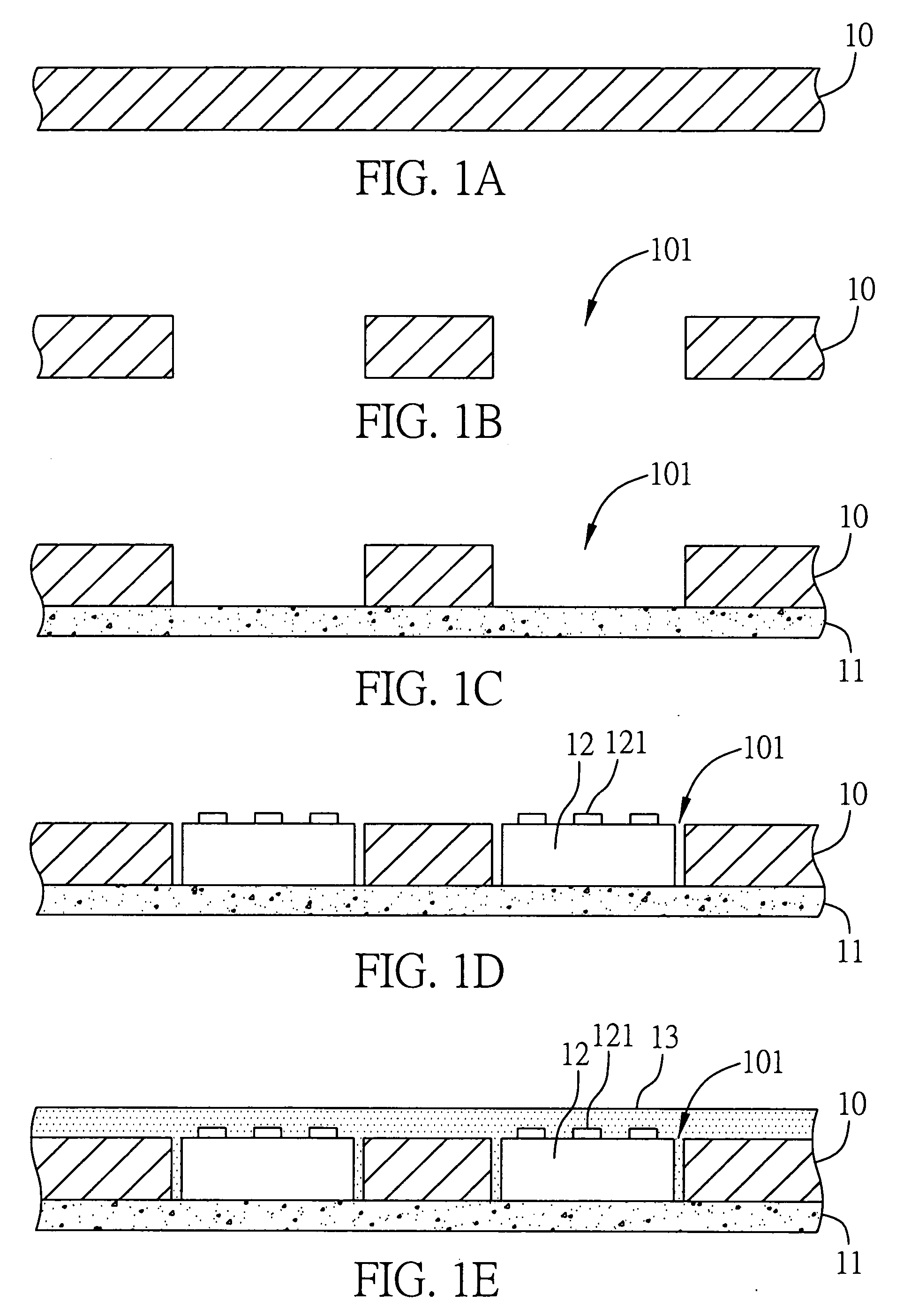
[0020]FIGS. 1A to 1E are cross-sectional schematic diagrams showing procedural steps of the method for fabricating a carrier structure integrated with a semiconductor element according to a first preferred embodiment of the present invention.

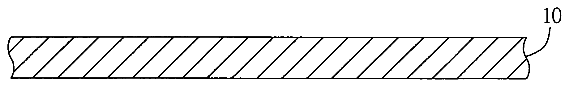
[0021] Referring first to FIG. 1A, a carrier 10 is provided, which can be an insulating board, printed circuit board, laminated substrate, or build-up substrate, etc.

[0022] Referring to FIG. 1B, the carrier 10 is formed with at least one opening 101 therein.

[0023] Referring to FIG. 1C, then a supporting substrate 11 is attached to a lower surface of the carrier 10 to temporarily seal the bottom of the opening 101. The supporting substrate 11 can be a film, dry film, tape, metal board, or insulating board, etc.

[0024] Referring to FIG. 1D, at least one semiconductor element 12 is embedded in the opening 101 of the carrier 10. The semiconductor element 12 can be a chip or a chip-type passive component with a plurality of electrode pads 121 form...

second preferred embodiment

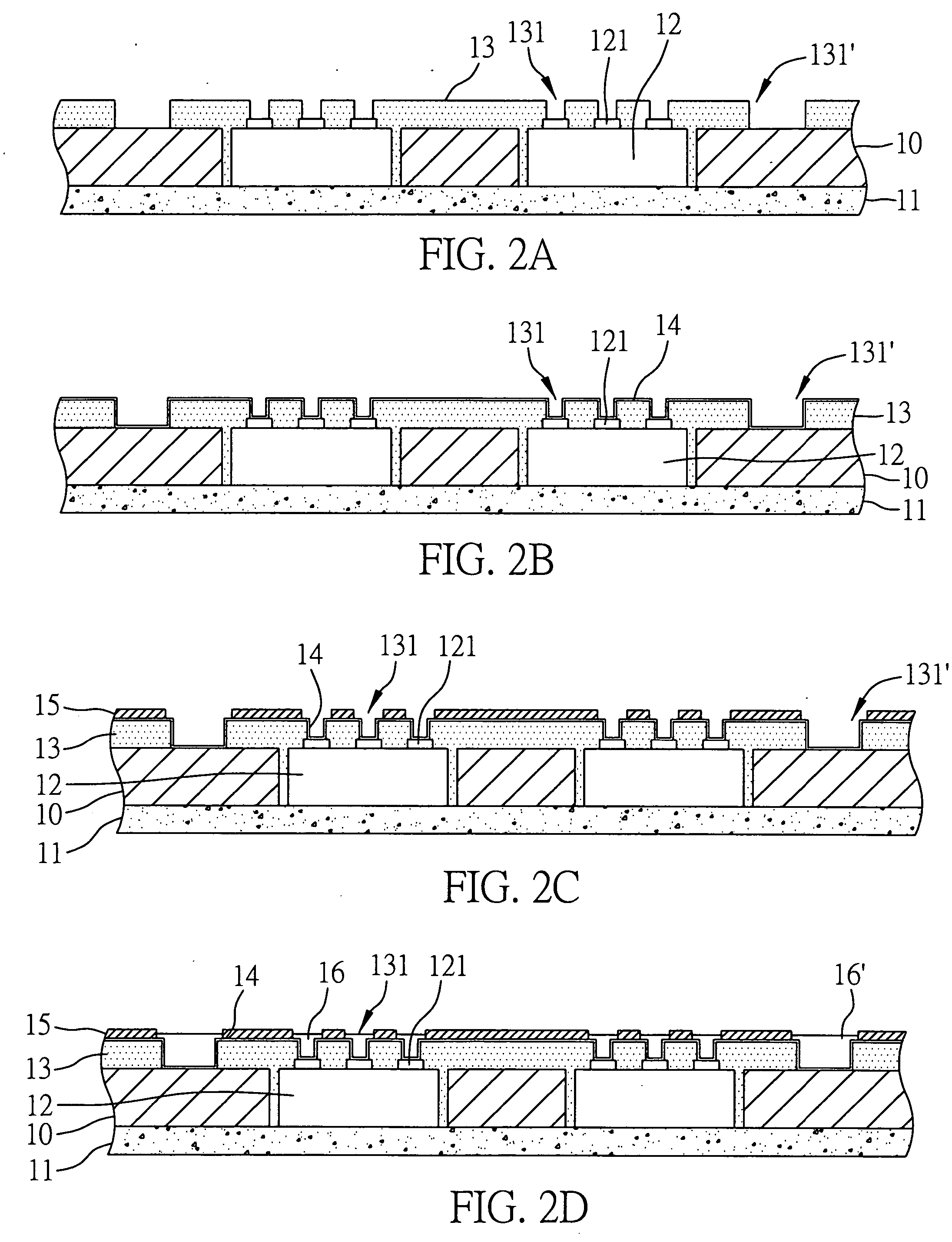
[0029]FIGS. 2A to 2F are cross-sectional schematic diagrams showing procedural steps of the method for fabricating a carrier structure integrated with a semiconductor element according to a second preferred embodiment of the present invention. In this second embodiment, the foregoing steps of FIGS. 1A to 1E are repeated and not to be further described here, which are followed by the steps shown in FIGS. 2A to 2F.

[0030] Referring to FIG. 2A, after the photosensitive insulating layer 13 is formed over the surface of the carrier 10 by coating or pressing (as shown in FIG. 1E), a patterning process is performed on the photosensitive insulating layer 13, such that recessed grooves 131, 131′ are formed in the photosensitive insulating layer 13, and electrode pads 121 of the semiconductor element 12 and predetermined portions on the surface of the carrier 10 are exposed via the recessed grooves 131, 131′ respectively. The recessed grooves 131, 131′ can be contact holes or circuit slots. T...


PUM

PropertyMeasurementUnit
photosensitiveaaaaaaaaaa
conductiveaaaaaaaaaa
heightaaaaaaaaaa

Abstract

A method for fabricating a carrier structure integrated with a semiconductor element is proposed. First, a carrier having at least one opening therein is provided, and at least one semiconductor element is embedded in the opening. Then, a photosensitive insulating layer is formed on the carrier and filled into a gap between the opening of the carrier and the semiconductor element, such that the semiconductor element is fixed in the opening. Subsequently, the photosensitive insulating layer is patterned, and build-up circuits are formed on the semiconductor element. By such arrangement, the overall fabrication processes are simplified and the fabrication cost can be reduced.

Description

FIELD OF THE INVENTION [0001] The present invention relates to methods for fabricating carrier structures integrated with semiconductor elements, and more particularly, to a method for embedding and fixing a semiconductor element in. BACKGROUND OF THE INVENTION [0002] Along with the evolution of semiconductor packaging technology, different types of packages for semiconductor elements have been developed. Such semiconductor package normally comprises a semiconductor chip mounted on and electrically connected to a substrate or lead frame, and an encapsulant made of a resin material for encapsulating the chip. [0003] The method for electrically connecting the semiconductor chip to the substrate or lead frame currently includes a wire-bonding technique or a flip-chip bonding technique. For either of a wire-bonded package or a flip-chip package, the semiconductor chip is formed with a plurality of bond pads thereon where the electrical connection is established. For example of the flip-...

Claims


Application Information

Patent Timeline
Patent Type & Authority Applications(United States)
IPC IPC(8): G03F7/00
CPCH01L21/568H01L2924/014H01L23/5389H01L24/24H01L24/82H01L2224/24227H01L2924/01013H01L2924/01029H01L2924/01074H01L2924/01082H01L2924/15153H01L2924/1517H01L2924/18162H01L21/6835H01L2924/01033H01L2924/01023
Inventor CHEN, CHI-MING
Owner PHOENIX PRECISION TECH CORP
Why Eureka
Try Eureka