Semiconductor device and semiconductor device unit

a semiconductor device and semiconductor technology, applied in the field of semiconductor device and semiconductor device unit, can solve the problems of affecting the operation of the device, the ductility of the semiconductor device, and the inability to mount such a semiconductor device freely in a limited small space in a compact apparatus, and achieve the effect of increasing the number of functions of the system, reducing the size, and increasing the density of the mounted elements

Inactive Publication Date: 2006-04-06
SHARP KK
View PDF28 Cites 65 Cited by
  • Summary
  • Abstract
  • Description
  • Claims
  • Application Information

AI Technical Summary

Benefits of technology

[0012] An object of the present invention is to provide a semiconductor device which makes both an increase in the number of functions of a system and an increase in the density of mounted elements through reduction in size possible.

Problems solved by technology

However, although it is possible to achieve an increase in density of integrated elements by using a semiconductor device in a thin film form that has been fabricated as described above, such a semiconductor device lacks flexibility and ductility and is fragile.
Therefore, it is difficult to mount such a semiconductor device freely in a limited small space in a compact apparatus, a portable apparatus, a wearable apparatus and the like.

Method used


Image

  • Semiconductor device and semiconductor device unit
  • Semiconductor device and semiconductor device unit
  • Semiconductor device and semiconductor device unit

Examples


first embodiment

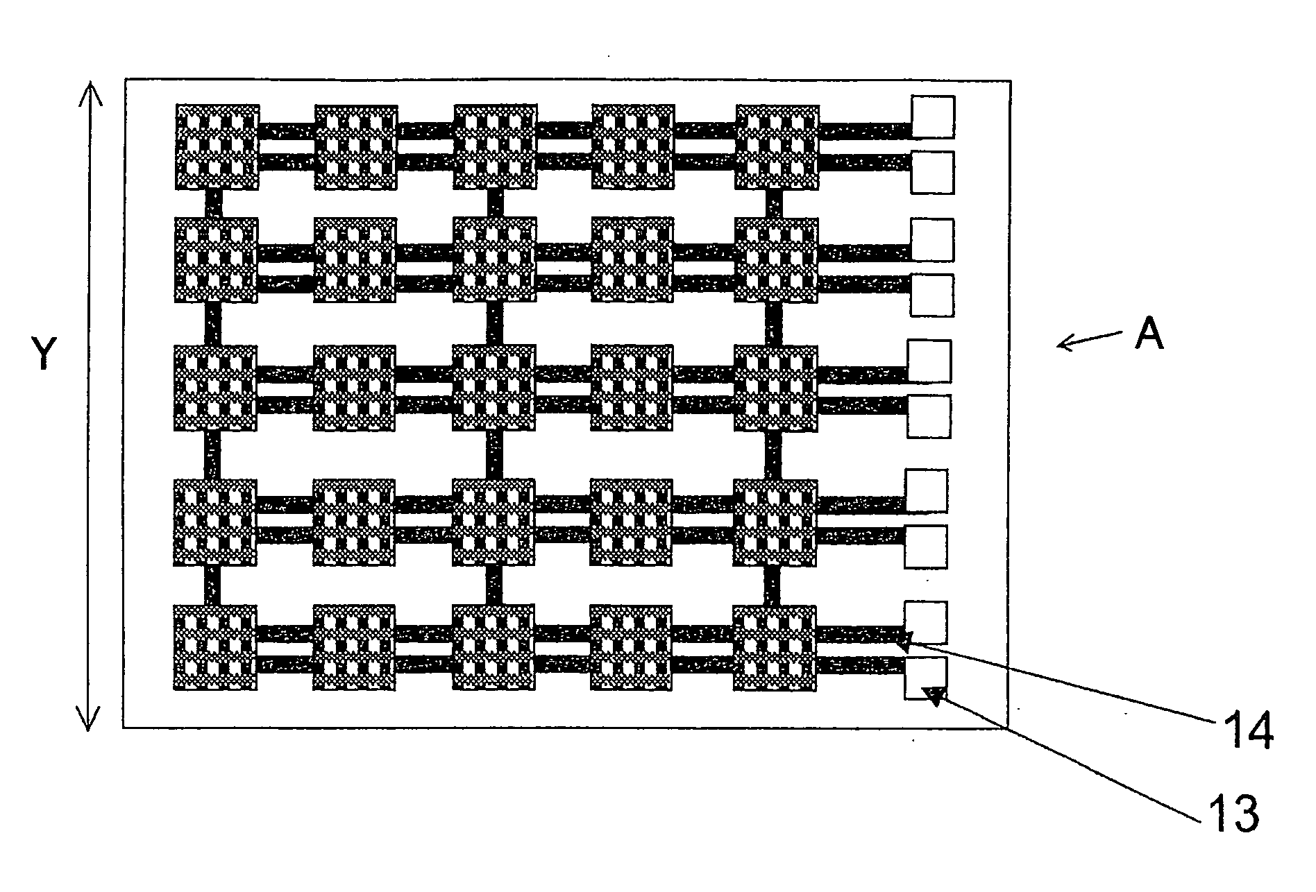
[0052]FIGS. 1A and 1B are a plan view and a lateral sectional view that illustrate a semiconductor device according to a first embodiment of the present invention.

[0053] A semiconductor device A of this embodiment includes a flexible substrate 11 which is rectangular in a plan view, a plurality of electrodes for external connections which are made of Al along a first end on the front surface of the flexible substrate 11, i.e., pad electrodes 13, a plurality of semiconductor elements 12 which are formed in matrix form on the front surface of the flexible substrate 11, and a plurality of wires 14 which are made of Cu for electrical connection between the semiconductor elements 12 and between the semiconductor elements 12 and the pad electrodes 13 on the front surface of the flexible substrate 11.

[0054] Next, a manufacturing method of the semiconductor device of this embodiment is described with reference to FIG. 1.

[0055] First, a plurality of pieces which are aligned in a straight ...

second embodiment

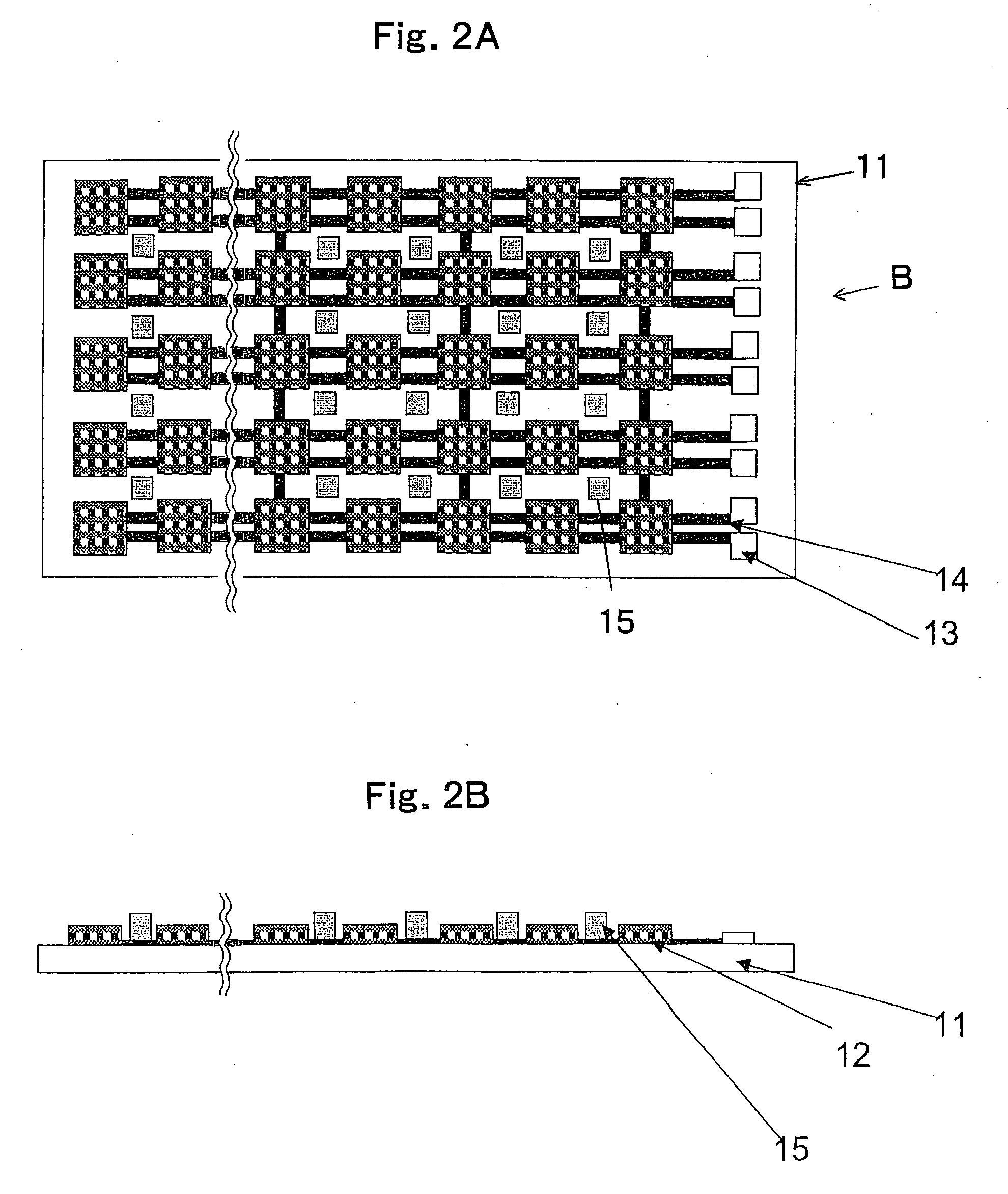
[0058]FIGS. 2A and 2B are a plan view and a lateral sectional view that illustrate a semiconductor device according to a second embodiment of the present invention.

[0059] A semiconductor device B of this embodiment is different from the semiconductor device of the first embodiment in that a plurality of protrusions 15 are formed in spaces between the respective semiconductor elements 12 and the wires 14 on the front surface of the flexible substrate 11, and the other configurations are the same as those in the first embodiment. An appropriate material can be selected for these protrusions 15 from plastics having insulating properties and metals having conductivity, in accordance with conditions such as adhesiveness to the flexible substrate 11 or required mechanical strength, and these protrusions may be made to adhere with an adhesive or a solder.

third embodiment

[0060]FIGS. 3A and 3B are a front view and a perspective view that illustrate a semiconductor device according to a third embodiment of the present invention.

[0061] A semiconductor device C of this embodiment is obtained by rolling and holding the semiconductor device of the first embodiment in a cylindrical form. At the time of the fabrication of this cylindrical semiconductor device, a method for rolling the flexible substrate 11 using a rod as a core can be used. The flexible substrate 11 can be rolled in a state where the pad electrodes 13 are exposed on the outside and, thereafter, the cylindrical form can be held be means of adhesion.

[0062] The flexible substrate 11 having a length of X and a width of Y before rolling is rolled into this cylindrical semiconductor device C having a diameter of approximately X / π.

[0063]FIG. 4 illustrates a state where a plurality of cylindrical semiconductor devices are arranged in proximity to each other. As illustrated in this figure, the ar...


PUM


Abstract

A semiconductor device, comprising: a flexible substrate; at least one semiconductor element; at least one electrode for external connection, the element and the electrode being formed on a front surface of the flexible substrate; and at least one wire formed on the front surface to electrically connect the element to the electrode, wherein at least a part of the flexible substrate has a curved form.

Description

CROSS-REFERENCE TO RELATED APPLICATION [0001] This application is related to Japanese application No. 2004-293787, filed on Oct. 6, 2004 whose priority is claimed under 35 USC § 119, the disclosure of which is incorporated by reference in its entirety. BACKGROUND OF THE INVENTION [0002] 1. Field of the Invention [0003] The present invention relates to a semiconductor device and a semiconductor device unit. More specifically, it relates to a mounting technique for a semiconductor device having flexibility. [0004] 2. Description of the Related Art [0005] The demand for miniaturization and portability of apparatuses like mobile telephones is growing stronger, and in addition, “wearable personal computers” have been announced. Furthermore, interfaces which directly recognize images and sounds, such as 3DMDs (see-through head-mount displays), CCD camera built-in HDs, earphone-type spectacles and earphone-type microphones have been proposed, and it is likely that the market for wearable a...

Claims


Application Information

Patent Timeline
Patent Type & Authority Applications(United States)
IPC IPC(8): H01L23/52
CPCH01L23/5387H01L25/0655H01L27/1214H01L27/14618H01L29/78603H01L2924/0002H01L2924/00
Inventor TOKUSHIGE, NOBUAKINISHIO, OSAMUAWAYA, NOBUYOSHI
Owner SHARP KK
Why Eureka
Try Eureka