System and method for the probing of a wafer

a technology of probing system and wafer, applied in the field of electronic component testing, can solve the problems of inability to achieve and maintain parallelism between the two planes of stack up control, inability to compensate for stack up variance of typical manipulating and docking system, and inability to achieve and maintain parallelism of these two planes by stack up control alone. achieve the effect of greatly reducing disadvantages and problems associated

Inactive Publication Date: 2006-04-06
TEXAS INSTR INC
View PDF5 Cites 18 Cited by
  • Summary
  • Abstract
  • Description
  • Claims
  • Application Information

AI Technical Summary

Benefits of technology

[0004] From the foregoing it may be appreciated by those skilled in the art that a need has arisen for a system and method for the probing of a wafer. In accordance with the present inve...

Problems solved by technology

Typical manipulating and docking systems do not compensate for stack up variances associated with component interchangeability within the testhead, probe card and prober.
Achieving and maintaining parallelism of these two planes by stack up control alone is impractical for systems that use vacuum to attach the ...

Method used


Image

  • System and method for the probing of a wafer
  • System and method for the probing of a wafer
  • System and method for the probing of a wafer

Examples


Embodiment Construction

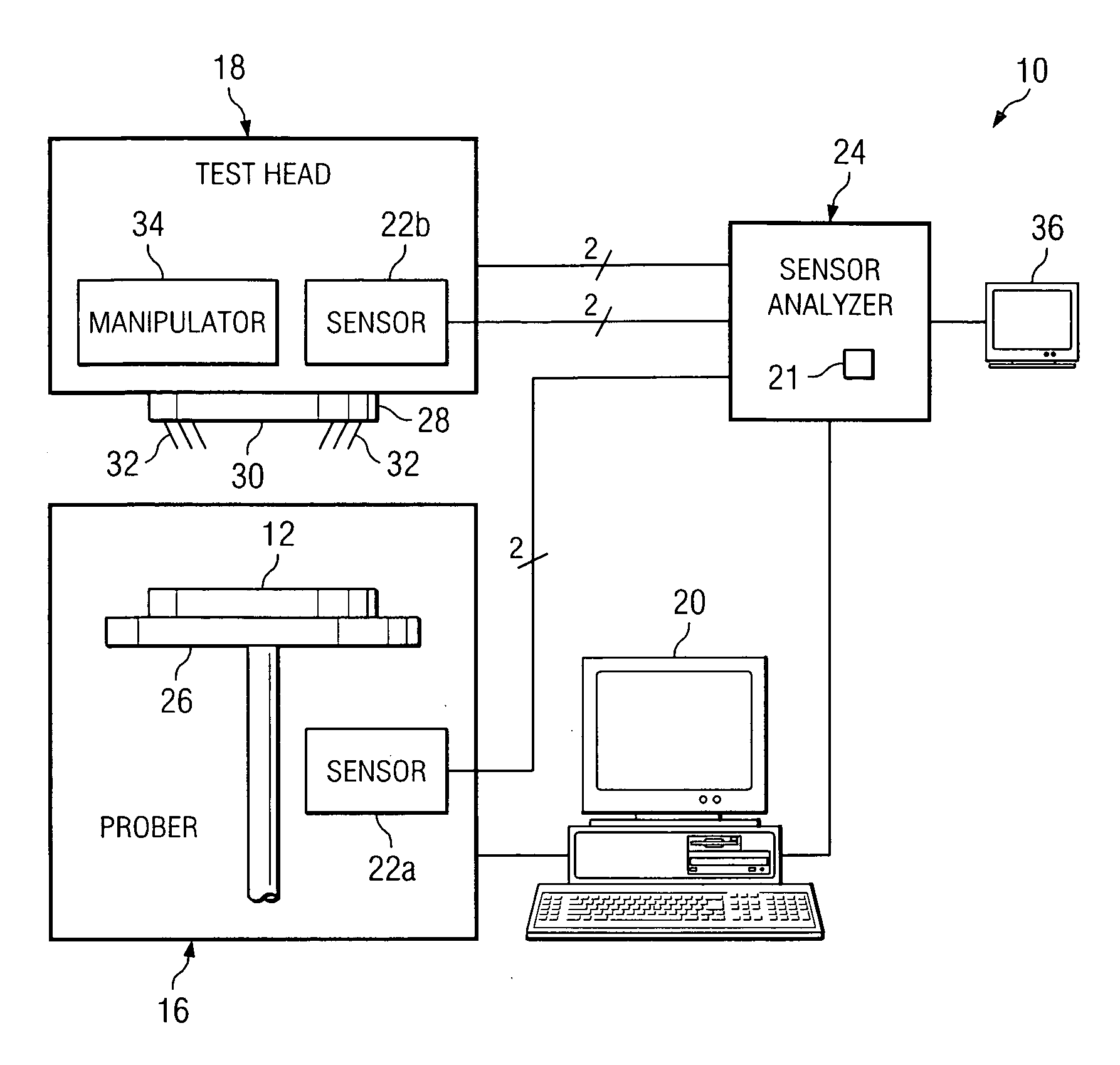
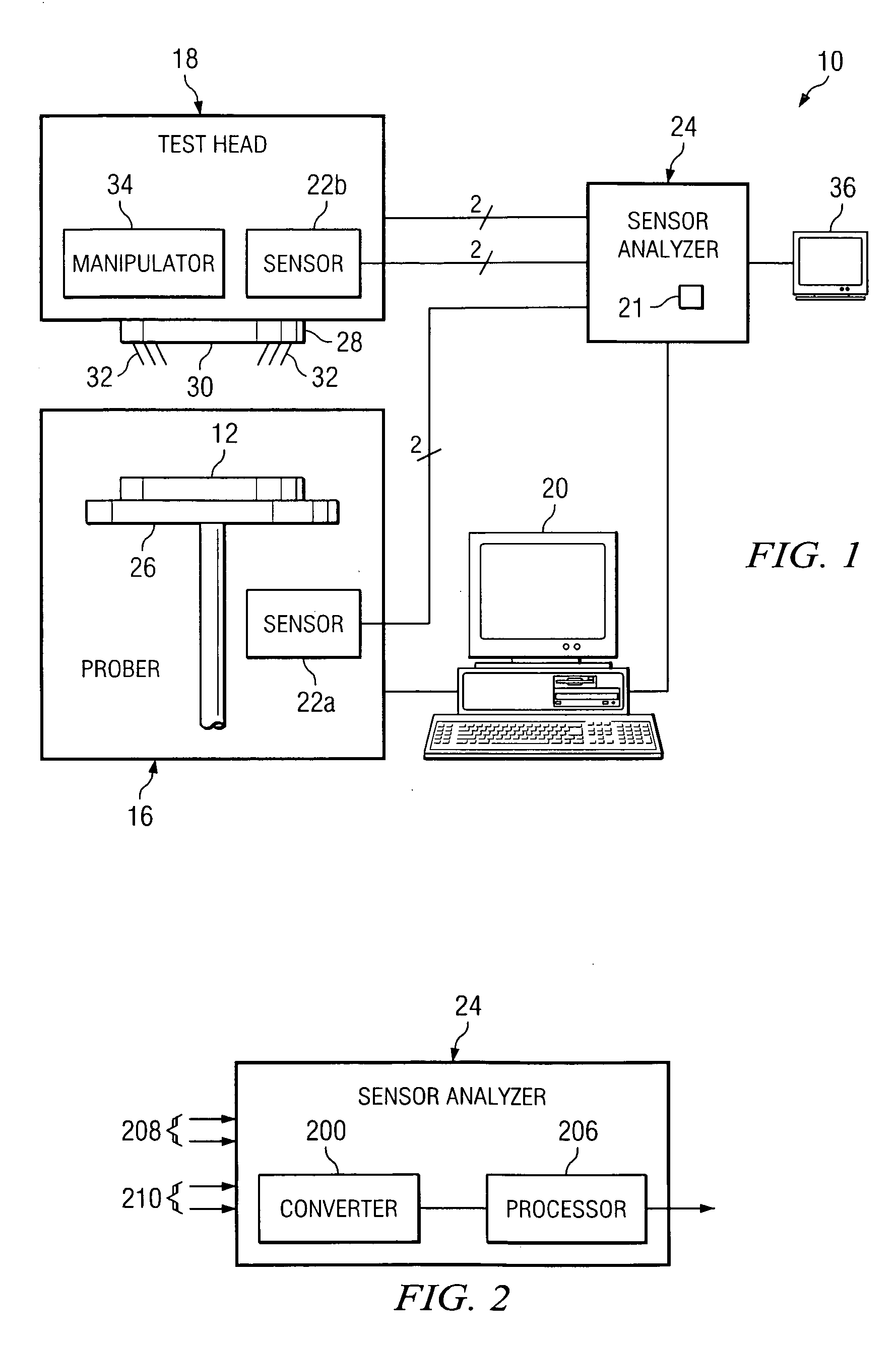
[0012]FIG. 1 is a block diagram of a system 10 for the probing of a wafer 12. In various embodiments, wafer 12 may include a thin polished slice of crystal material sliced from a crystal cylinder grown for the purpose of semiconductor fabrication. In a typical fabrication technology, a wafer provides the foundation on which a semiconductor device may be created. The semiconductor device may be created on the surface of the wafer using a variety of techniques and procedures, such as layering, photolithographic patterning, doping through implantation of ionic impurities, and heating. The starting material may comprise silicon, gallium arsenide, or other suitable substrate material. As will be described in further detail below, system 10 includes a prober 16, a testhead 18, and a controller 20. In particular embodiments, the different components of system 10 cooperate to read data from, write data to, or otherwise gather information about each die on wafer 12. For the efficient and acc...


PUM


Abstract

According to one embodiment of the invention, a method for probing a wafer includes positioning a testhead relative to a prober supporting a wafer in a testing position. The method also includes receiving at least one prober signal identifying the angular position of the prober and at least one testhead signal identifying the angular position of the testhead. The at least one prober signal and the at least one testhead signal are processed to determine if the testhead is substantially parallel with the prober, and output is provided to allow for adjustment of the position of the testhead in response to determining that the testhead is not substantially parallel with the prober.

Description

TECHNICAL FIELD OF THE INVENTION [0001] This invention relates in general to the testing of electronic components, and more particularly to a system and method for the probing of a wafer. BACKGROUND OF THE INVENTION [0002] An array of die, which may include integrated circuits and their components, are typically supported on a wafer during various semiconductor fabrication processes. At various stages during fabrication processes, it may be desirable to perform testing on each die to read information from each die, write information to each die, or otherwise gather information about each die and components on each die. During testing, the wafer is typically loaded into a prober that operates to sequentially align each die on the wafer with the test equipment. To perform testing on each die of the wafer, the test equipment typically includes a testhead that is positioned and locked proximate the prober in an optimum testing position. This positioning and locking operation is known as...

Claims


Application Information

Patent Timeline
IPC IPC(8): G01R31/26
CPCG01R31/2891
Inventor GIBBS, BYRON H.MCCLANAHAN, ADOLPHUS E.BALL, PHILLIP H.
Owner TEXAS INSTR INC
Why Eureka
Try Eureka