Multilevel phase-change memory, manufacturing and status transferring method thereof

a phase-change memory and multi-level technology, applied in the direction of digital storage, electrical equipment, instruments, etc., can solve the problems of difficult control of multi-state, fast storage operation and long storage time, writing error, etc., to reduce the area of one bit, increase the memory density, and eliminate operations

Inactive Publication Date: 2006-04-13
IND TECH RES INST
View PDF14 Cites 94 Cited by
  • Summary
  • Abstract
  • Description
  • Claims
  • Application Information

AI Technical Summary

Benefits of technology

[0023] According to the object of the invention, the phase change memory has the advantage of reducing the area of one bit. Thus, the memory density is increased.
[0024] According to the object of the invention, the phase change memory has the advantage of direct writing and erasing operations.
[0025] According to the object of the invention, the phase change memory has the advantage of shortening time for writing and erasing operations.
[0026] According to the object of the invention, the phase change memory has the advantage of reducing complexity for fabricating the devices. Additional masks are not necessary for the process of the memory.

Problems solved by technology

Phase change memory meets the need for large and fast storage operation and long storage time.
However, the solution may have the problem of small current separation such that writing error occurs due to the current offset.
Besides, the multi-state is difficult to control after continuous operations due to the heating effects.
Furthermore, operation voltage decreases gradually.

Method used


Image

  • Multilevel phase-change memory, manufacturing and status transferring method thereof
  • Multilevel phase-change memory, manufacturing and status transferring method thereof
  • Multilevel phase-change memory, manufacturing and status transferring method thereof

Examples


Embodiment Construction

[0038] Reference will now be made in detail to an embodiment of the invention, examples of which are illustrated in the accompanying drawings. Reference in the specification to “one embodiment” or “an embodiment” means that a particular feature, structure, or characteristic described in connection with the embodiment is included in at least one embodiment of the invention. The phrase “in one embodiment” in various places in the specification does not necessarily refer to the same embodiment.

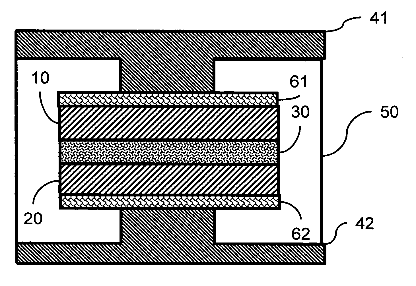
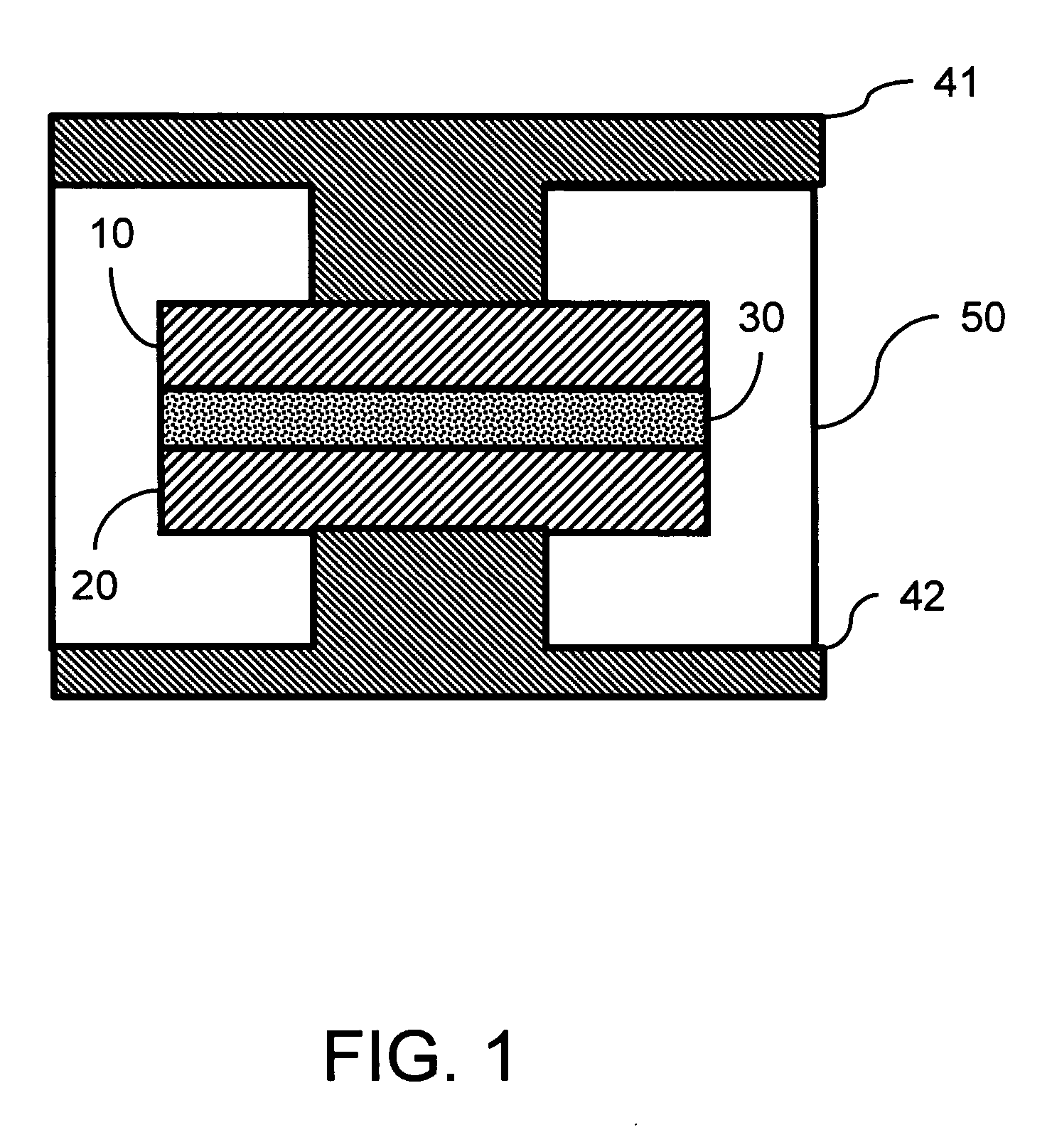
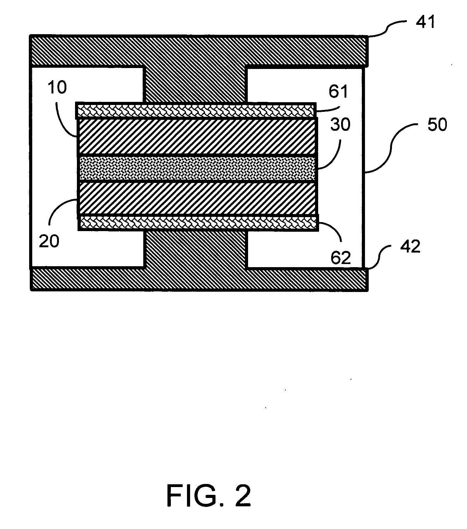
[0039] Refer to FIG. 1, which illustrates the structure of the phase change memory of the invention. In the embodiment, the phase change memory includes a first phase change layer 10, a second phase change layer 20, an intermediate layer 30, a first electrode 41 and a second electrode 42. The first phase change layer 10 and the second phase change layer 20 are formed on two surfaces of the intermediate layer 30 by a semiconductor process. The first electrode 41 is formed on another side of the f...


PUM


Abstract

A multilevel phase-change memory, manufacturing method and status transferring method thereof. The phase-change memory includes two phase-change layers and electrodes, which are configured in a series structure to form a memory cell. A current-drive mode is employed to control and drive the memory such that multilevel memory states may be achieved by imposing different current levels. The provided multilevel phase-change memory has more bits and higher capacity than that of the memory with a single phase-change layer. Furthermore, the series structure may reduce the cell area and the device volume.

Description

[0001] This application claims the benefit of Taiwan Patent Application No. 93130598, filed on Oct. 8, 2004, which is hereby incorporated by reference for all purposes as if fully set forth herein. BACKGROUND OF THE INVENTION [0002] 1. Field of Invention [0003] The invention relates to a semiconductor memory device, and more particularly to a semiconductor memory device with a multi-level memory state. [0004] 2. Related Art [0005] Memory is widely used in most electronic devices. Most are DRAM, SRAM, or Flash memory. Application and architecture of electric devices determines the usage of the memory and the required capacity. Development of memory technology, such as FeRAM, MRAM and phase change memory, is on-going. [0006] Phase change semiconductor memory stores data through resistance variation caused by the phase change of materials. Regarding the phase materials, in the 1960s, S. R. Ovshinsky of the U.S. company ECD discovered that crystallization and amorphization of chalcogeni...

Claims


Application Information

Patent Timeline
Patent Type & Authority Applications(United States)
IPC IPC(8): G11C7/00
CPCG11C11/56G11C11/5678G11C13/0004H01L45/06H01L45/1233H01L45/126H01L45/144H10N70/231H10N70/826H10N70/8413H10N70/8828
Inventor WANG, WEN-HANLI, CHIEN-MINGSHEN, KUEI-HUNG
Owner IND TECH RES INST
Why Eureka
Try Eureka