Address buffer circuit and method for controlling the same

a buffer circuit and address technology, applied in the direction of information storage, static storage, digital storage, etc., can solve the problems of increasing power consumption, power consumption, and limitation of chip select signal use, and achieve the effect of reducing power consumption

Inactive Publication Date: 2006-04-13
SAMSUNG ELECTRONICS CO LTD
View PDF8 Cites 1 Cited by
  • Summary
  • Abstract
  • Description
  • Claims
  • Application Information

AI Technical Summary

Benefits of technology

[0027] An embodiment of the invention provides a (gated) address buffer and a method for controlling the same, which are capable of reducing power consumption by disabling the address buffer during no-operation states of a semiconductor memory device.
[0028] Another embodiment of the invention provides an address buffer circuit and a method for controlling the same, which are capable of reducing or minimizing power consumption in a semiconductor memory device by reducing a signal buffered and output by an address buffer during a ‘no operation’ state (NOP command) in which memory cells are not accessed. Standard memory control signals are logically combined to generate a control signal for enabling and disabling the address buffer.

Problems solved by technology

This results in power consumption due to current flowing through the address buffer 1.
Further, the internal address signal (int.an), which is buffered and output in the address buffer 1, is input to all chips, resulting in increased power consumption.
Thus, there is a limitation in using a chip select signal (cs) at a subsequent stage of the address buffer to reduce power consumption.
Thus, unnecessary current still flows, increasing power consumption in the semiconductor memory device.

Method used


Image

  • Address buffer circuit and method for controlling the same
  • Address buffer circuit and method for controlling the same
  • Address buffer circuit and method for controlling the same

Examples


Embodiment Construction

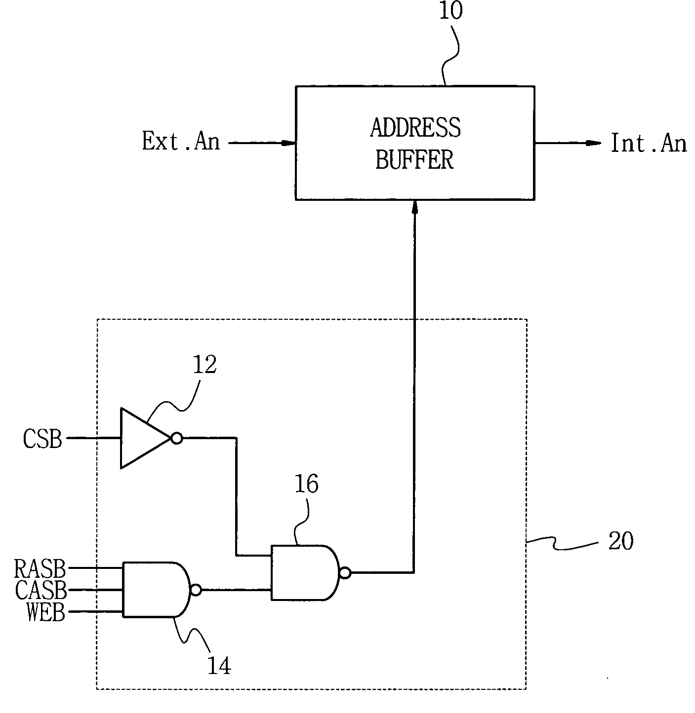
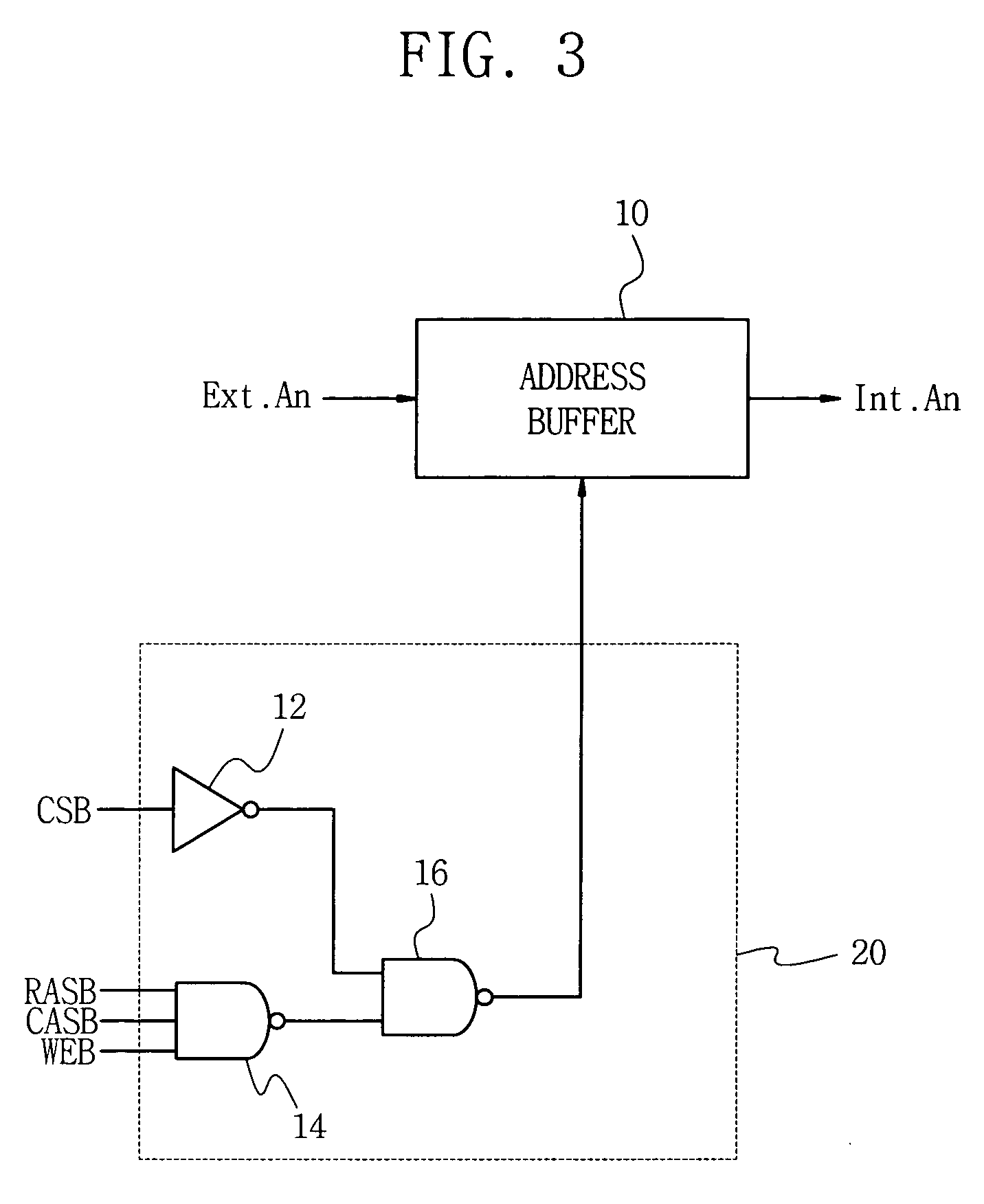
[0050]FIG. 3 is a schematic diagram of an address buffer circuit comprising an address buffer control unit according to an embodiment of the present invention.

[0051] Referring to FIG. 3, there are shown an address buffer 10 that receives and buffers an external address signal and outputs an internal address signal, an external address signal (ext.an) input to the address buffer 10, an internal address signal (Int.an) buffered by and output from the address buffer 10, and an address buffer control unit 20 for controlling the address buffer 10. The address buffer control unit 20 shown in FIG. 3 consists essentially of a combinatorial logic circuit that combines memory control signals (e.g., RASB, CASB, WEB) and a chip select signal (CS). The address buffer control unit 20 includes an inverter 12, a first NAND-gate 14, and a second NAND-gate 16.

[0052] Memory control signals, including a chip select signal (CSB), a row address strobe (RASB), a column address strobe (CASB), a write ena...


PUM


Abstract

An address buffer circuit for a semiconductor memory device wherein an address buffer is enabled (to output an internal address signal) in response to a first level of a control signal and, but is disabled in response to a second level of the control signal. An address buffer control unit generates the control signal at the second level in ‘no operation’ state (NOP command) in which the semiconductor memory device does not perform data accessing operations and generates the control signal at the first level while the semiconductor memory device performs data accessing operations, thereby reducing or minimizing the output of an internal address buffered and output by the address buffer at and thus reducing power consumption during no-operation states of the semiconductor memory device.

Description

CROSS-REFERENCE TO RELATED APPLICATION [0001] This application claims the priority under 35 USC § 119 of Korean Patent Application No. 2004-10-0081561, filed Oct. 13, 2004, which is incorporated herein by reference in its entirety. BACKGROUND OF THE INVENTION [0002] 1. Technical Field [0003] The present invention relates to semiconductor memory devices, and more particularly, to address buffers for semiconductor memory devices. [0004] 2. Discussion of the Related Art [0005] Memory chip designers and users seek semiconductor memory chips capable of satisfying high density integration, high-speed operation, and low power consumption. [0006] Generally, transistor-transistor logic (TTL) or complementary metal oxide semiconductor (CMOS) technologies have been used for chips that communicate data with dynamic random access memories (DRAMs). TTL has a noise margin narrower than that of CMOS. In particular, DRAMs connected to such chips are required to withstand variations of power supply v...

Claims


Application Information

Patent Timeline
Patent Type & Authority Applications(United States)
IPC IPC(8): G11C8/00
CPCG11C8/06G11C7/109G11C7/22G11C8/18G11C11/4076G11C11/4093
Inventor KIM, SUNG-HOONKIM, JOUNG-YEAL
Owner SAMSUNG ELECTRONICS CO LTD
Why Eureka
Try Eureka