Methods for fabricating solid state image sensor devices having non-planar transistors

a solid-state image sensor and transistor technology, applied in the direction of transistors, solid-state devices, radiation control devices, etc., can solve the problems of not allowing random access to unit pixels, high cost of ccd image sensor devices, and high power consumption, so as to reduce the effects of image lag and dark curren

Active Publication Date: 2006-04-20
SAMSUNG ELECTRONICS CO LTD
View PDF8 Cites 72 Cited by
  • Summary
  • Abstract
  • Description
  • Claims
  • Application Information

AI Technical Summary

Benefits of technology

[0007] Exemplary embodiments of the invention generally include CMOS image sensor devices. More specifically, exemplary embodiments of the invention include methods for fabricating CMOS image sensor devices comprising active pixel sensors that are constructed with non-planar transistors having vertical gate electrodes and channels, which minimize the effects of image lag and dark current.

Problems solved by technology

In contrast, CCD image sensor devices are expensive to fabricate, typically require 2, 3 or more supply voltages at different clock speeds with significantly higher power consumption, and do not allow random access to unit pixels.
Conventional solid state CMOS image sensors, however, can suffer from low sensitivity and various sources of noise resulting in degraded performance.
For example, some conventional CMOS image sensors are highly susceptible to noise such as dark current.
Dark current is typically generated as a result of surface damage (e.g., dangling silicon bonds) to the active silicon regions of the unit pixel, such as the photodiode region, resulting from manufacturing processes such as gate and spacer etching steps.
In addition, dark current can be generated as a result of damage to the silicon at the interface between an isolation region and the active silicon region.
As a result, dark current can result in reduced pixel sensitivity and lower the dynamic range of the image sensor device.
Moreover, CMOS image sensors can suffer from a phenomenon known as image lag.
Moreover, image lag can result from an incomplete charge transfer from a photodiode to a sensing node of a given pixel.
In this regard, as CMOS image sensor devices are designed to operate with lower supply voltages to meet requirements for decreased power consumption, the ability to minimize image lag (due to incomplete charge transfer and reset) becomes more problematic.

Method used


Image

  • Methods for fabricating solid state image sensor devices having non-planar transistors
  • Methods for fabricating solid state image sensor devices having non-planar transistors
  • Methods for fabricating solid state image sensor devices having non-planar transistors

Examples


Embodiment Construction

[0035] Exemplary CMOS image sensor devices and methods for fabricating such devices according to exemplary embodiments of the invention will now be described more fully with reference to the accompanying drawings. It is to be understood that the drawings are merely schematic depictions where the thickness and dimensions of various components, layers and regions are not to scale, but rather exaggerated for purposes of clarity. It is to be further understood that when a layer is described herein as being “on” or “over” another layer or substrate, such layer may be directly on the other layer or substrate, or intervening layers may also be present. It is to be further understood that the same reference numerals used throughout the drawings denote elements that are the same or similar or have the same or similar functions.

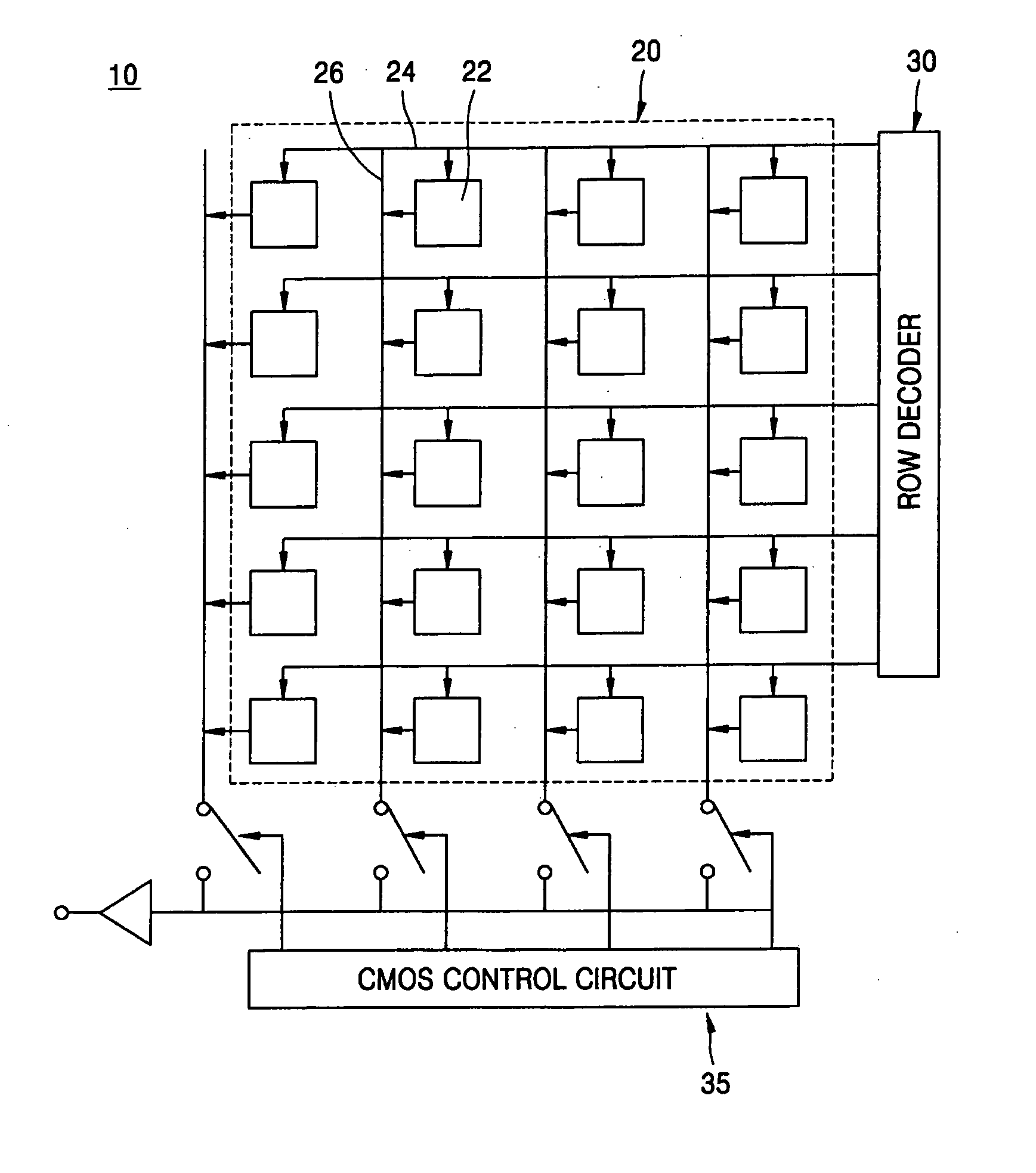
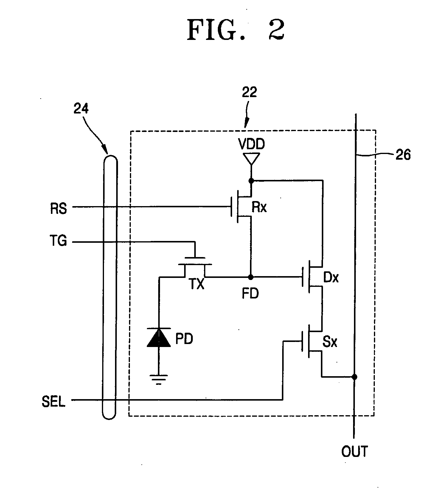
[0036]FIG. 1 is a high-level block diagram of a solid state CMOS image sensor device according to an exemplary embodiment of the invention. In particular, FIG. 1 illu...


PUM


Abstract

Methods for fabricating CMOS image sensor devices are provided, wherein active pixel sensors are constructed with non-planar transistors having vertical gate electrodes and channels, which minimize the effects of image lag and dark current.

Description

CROSS-REFERENCE TO RELATED APPLICATION [0001] This application claims priority to Korean Patent Application No. 10-2004-83968, filed on Oct. 20, 2004, which is fully incorporated herein by reference. TECHNICAL FIELD OF THE INVENTION [0002] The present invention relates generally to solid-state image sensor devices and, more specifically, to methods for fabricating CMOS image sensor devices comprising active pixel sensors that are constructed with non-planar transistors having vertical gate electrodes and channels, which minimize the effects of image lag and dark current. BACKGROUND [0003] Various types of solid state imaging devices have been developed, which primarily include charge-coupled devices (CCDs) and complementary metal oxide semiconductor (CMOS) image sensor devices, as well as hybrid image sensors that based on a combination of CCD and CMOS image sensor designs. In general, CCD and CMOS solid state imaging sensors CCD image sensors operate based on the “photoelectric eff...

Claims


Application Information

Patent Timeline
Patent Type & Authority Applications(United States)
IPC IPC(8): H01L21/00
CPCH01L27/14603H01L27/14609H01L27/1463H01L27/14612H01L27/14654H01L27/14689H01L27/14643H01L27/146H01L31/10
Inventor LYU, JEONG HO
Owner SAMSUNG ELECTRONICS CO LTD
Why Eureka
Try Eureka