Semiconductor structure for providing strained crystalline layer on insulator and method for fabricating same

a technology of insulator and crystalline layer, which is applied in the direction of semiconductor devices, basic electric elements, electrical appliances, etc., can solve the problems of high number of threading dislocations in the layer, high cost, and the above method is limited to a germanium content below 40%, and achieves a simple and relatively easy method of fabricating. , the effect of low crystal defect density

Active Publication Date: 2006-04-27
SOITEC SA
View PDF4 Cites 2 Cited by
  • Summary
  • Abstract
  • Description
  • Claims
  • Application Information

AI Technical Summary

Benefits of technology

[0011] The present invention provides a semiconductor structure having a high-strained crystalline layer with a low crystal defect density and a simple and relatively easy method for fabricating such a semiconductor structure.
[0020] The present invention also provides a simple and relatively easy method for fabricating a semiconductor structure with a high crystal quality and a high strained crystal semiconductor layer on top of an insulator. Such a method includes growing a crystalline epitaxial first layer, comprising a graded buffer layer and a substantially relaxed layer, on a substrate that includes a first material of at least one of germanium or a Group(III)-Group(V)-semiconductor, wherein the buffer layer contacts the first material; providing a further layer on the relaxed layer; and providing a weakened zone, for example by implanting atomic species, in the first layer to facilitate transfer of at least the further layer.

Problems solved by technology

Increasing germanium content of the graded GeSi layer causes cracks and a high number of threading dislocations to occur in the layer.
The process of growing a relaxed SiGe layer is very complex.
Furthermore, the above method is limited to a germanium content below 40% when a crystal defect density below 104 cm−2 is targeted.
This resulting structure, however, has a critical disadvantage in that the strain of the strained silicon layer on top of the SiGe layer cannot be increased to a value of commercial importance.

Method used


Image

  • Semiconductor structure for providing strained crystalline layer on insulator and method for fabricating same
  • Semiconductor structure for providing strained crystalline layer on insulator and method for fabricating same
  • Semiconductor structure for providing strained crystalline layer on insulator and method for fabricating same

Examples


first embodiment

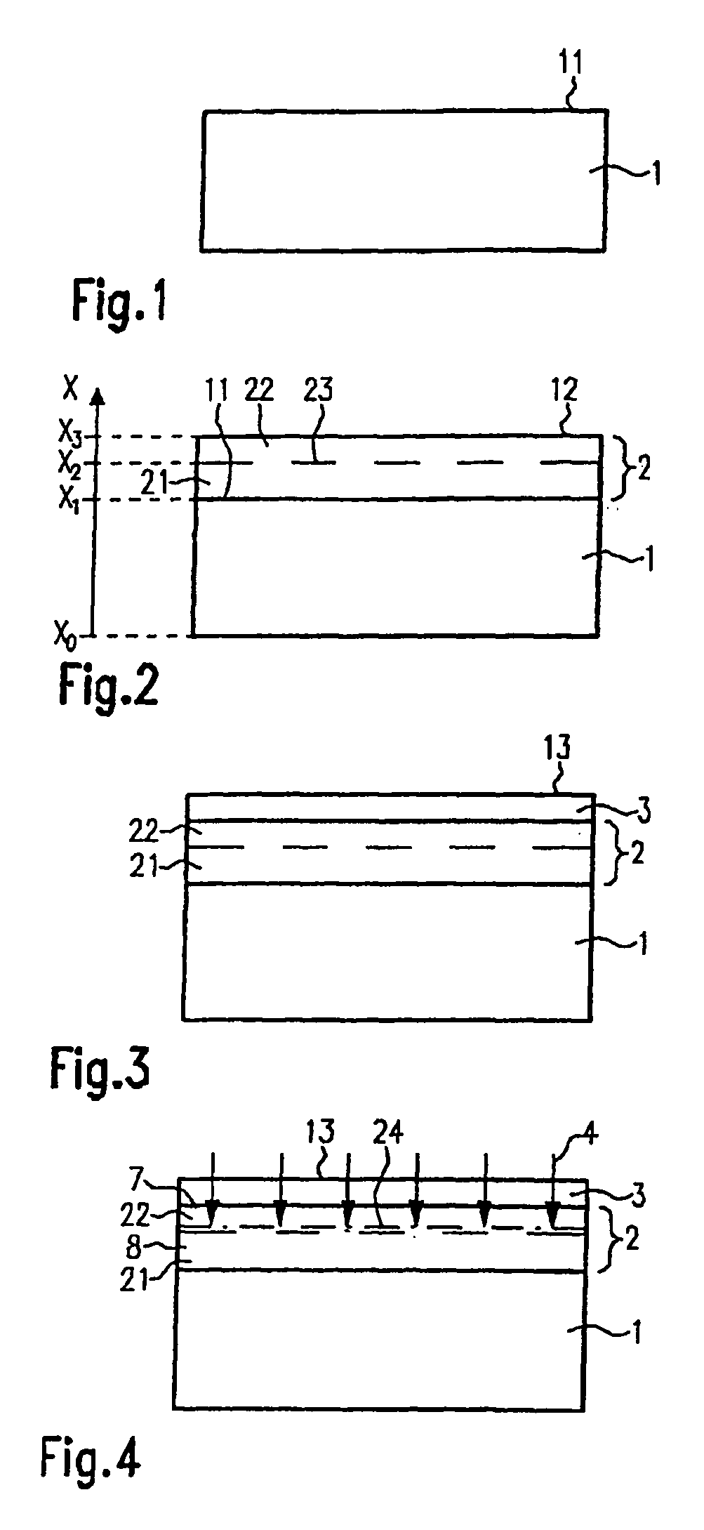
[0044]FIG. 2 illustrates the first step of the first embodiment wherein a first crystalline epitaxial layer 2 is grown on the semiconductor donor substrate 1 shown in FIG. 1. The first crystalline epitaxial layer 2 consists of a composition of germanium and silicon forming a GeSi layer. The GeSi layer 2 is deposited directly onto the upper surface 11 of the germanium wafer 1. In yet another embodiment, a seed layer of Ge can be deposited onto the upper surface 11 prior to growing the GeSi layer 2.

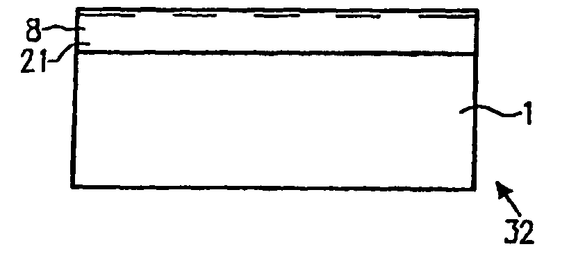
[0045] The GeSi layer 2 consists of two layers, a graded buffer GeSi layer 21 (x1 to x2) and a relaxed GeSi layer 22 (x2 to x3). The graded buffer GeSi layer 21 has a silicon concentration of about 0% near the surface 11 of the germanium wafer 1. The silicon content of the buffer GeSi layer 21 increases gradually beginning from the surface 11 of the germanium wafer 1 up to a level 23 where the silicon content of the GeSi layer is about 20% to 60%. Consequently, the germanium content of the ...

second embodiment

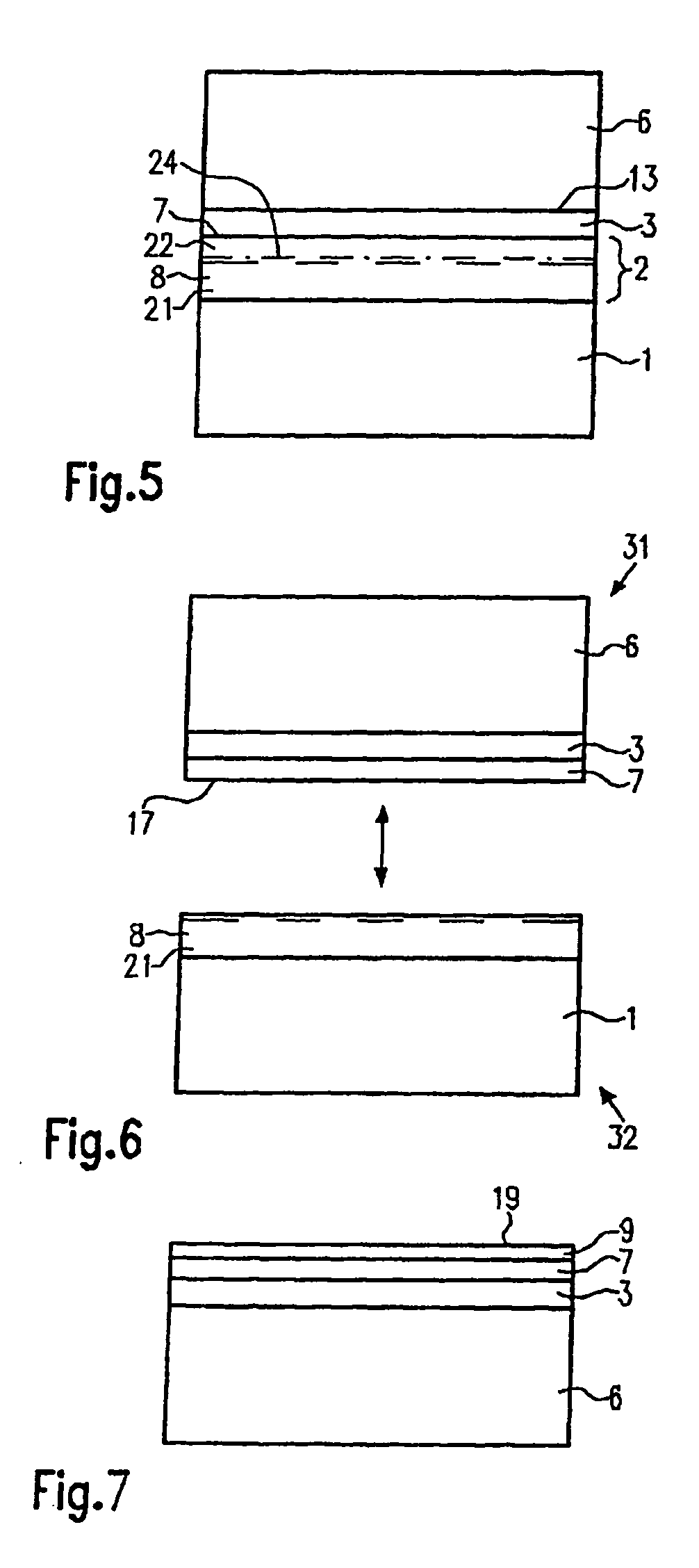
[0055] FIGS. 8 to 14 illustrate steps of a method according to the present technique. The same reference numerals used in FIGS. 8 to 13 are used in FIGS. 1 to 7 to indicate the same parts and components.

[0056]FIG. 8 shows a semiconductor substrate 1 which is used in a first step of the second embodiment of the present invention. The semiconductor substrate 1 is a single crystal germanium wafer and has an upper surface 11.

[0057]FIG. 9 shows the first step of the second embodiment of the present invention. In the first step, a first crystalline epitaxial layer is grown on the upper surface 11 of a germanium wafer 1. As mentioned with reference to FIGS. 1 to 7, in another embodiment a Group(III)-Group(V)-semiconductor or a substrate having an epitaxial surface layer of Ge or Group(III)-Group(V)-semiconductor layer can be used instead of the Ge wafer. The first crystalline epitaxial layer 2 is a GeSi layer consisting of a graded buffer GeSi layer 21 and a relaxed GeSi layer 22. The gra...


PUM

PropertyMeasurementUnit
thickaaaaaaaaaa
temperatureaaaaaaaaaa
thicknessaaaaaaaaaa

Abstract

A method for fabricating a semiconductor structure having a high-strained crystalline layer with a low crystal defect density is disclosed. The structure includes a substrate having a first material comprising germanium or a Group(III)-Group(V)-semiconductor or alloy thereof. In addition, a crystalline epitaxial first layer, comprising a graded buffer layer and a substantially relaxed layer, is provided. The buffer layer is sufficiently relaxed to provide relaxation of the substantially relaxed layer deposited thereon. A further layer may be provided on the first layer, and the transfer of at least the further layer is facilitated by providing a weakened zone in the first layer.

Description

CROSS-REFERENCE TO RELATED APPLICATIONS [0001] This application is a divisional of application Ser. No. 10 / 763,978 filed Jan. 22, 2004, and claims the benefit of U.S. provisional application 60 / 485,997 filed Jul. 9, 2003 and 60 / 485,998 filed Jul. 9, 2003, the entire content of each application mentioned above is expressly incorporated herein by reference thereto.BACKGROUND [0002] The present invention relates to a semiconductor structure having a strained crystalline layer formed on a single crystal substrate or on an insulator and further to a method for fabricating such a semiconductor structure. [0003] Strained, thin semiconductor layers, such as silicon layers, have enhanced electron and hole mobility characteristics which are advantageous for improving speed or decreasing power requirements of electronic devices. Because their use can lead to high performance devices having high speed and low power consumption, such layers are of interest in nearly all parts of microelectronics...

Claims


Application Information

Patent Timeline
Patent Type & Authority Applications(United States)
IPC IPC(8): H01L21/30H01L21/762
CPCH01L21/76254H01L21/76259
Inventor AULNETTE, CECILEDUPONT, FREDERICMAZURE, CARLOS
Owner SOITEC SA
Why Eureka
Try Eureka