Method of dividing wafer

a technology of dividing devices and wafers, applied in the direction of basic electric elements, semiconductor/solid-state device manufacturing, electric apparatus, etc., can solve the problems of deteriorating quality, reducing the die strength of the devices constituting the wafer, and not being efficient, so as to improve productivity, the effect of not deteriorating the quality of the device and not reducing the die strength

Inactive Publication Date: 2006-04-27
DISCO CORP
View PDF2 Cites 50 Cited by
  • Summary
  • Abstract
  • Description
  • Claims
  • Application Information

AI Technical Summary

Benefits of technology

[0010] According to the present invention, the wafer is divided into individual devices relying upon the plasma etching and grinding instead of cutting by means of a cutting blade. Therefore, chippings cannot cause in the devices, the die strength of the devices does not decrease, and the quality thereof is not deteriorated. Further, the grooves-forming step is capable of forming grooves simultaneously in all streets by plasma etching, which is very efficient improving the productivity. Moreover, the front surface of the wafer is coated with a resist film by using an exposure device and a device for forming a resist film that have been used in a device-forming step of forming the devices on the wafer (p

Problems solved by technology

At the time of dicing, however, the cutting blade rotating at a high speed bites into the street of the wafer whereby the devices are partly cut away due to the crushing force of the cutting blade and, hence, the die strength of the devices constituting the wafer decreases to deteriorate the quality.
At the time of dicing, further, the cutt

Method used


Image

  • Method of dividing wafer
  • Method of dividing wafer
  • Method of dividing wafer

Examples


Embodiment Construction

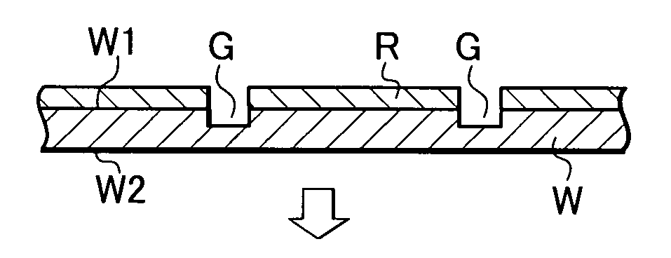
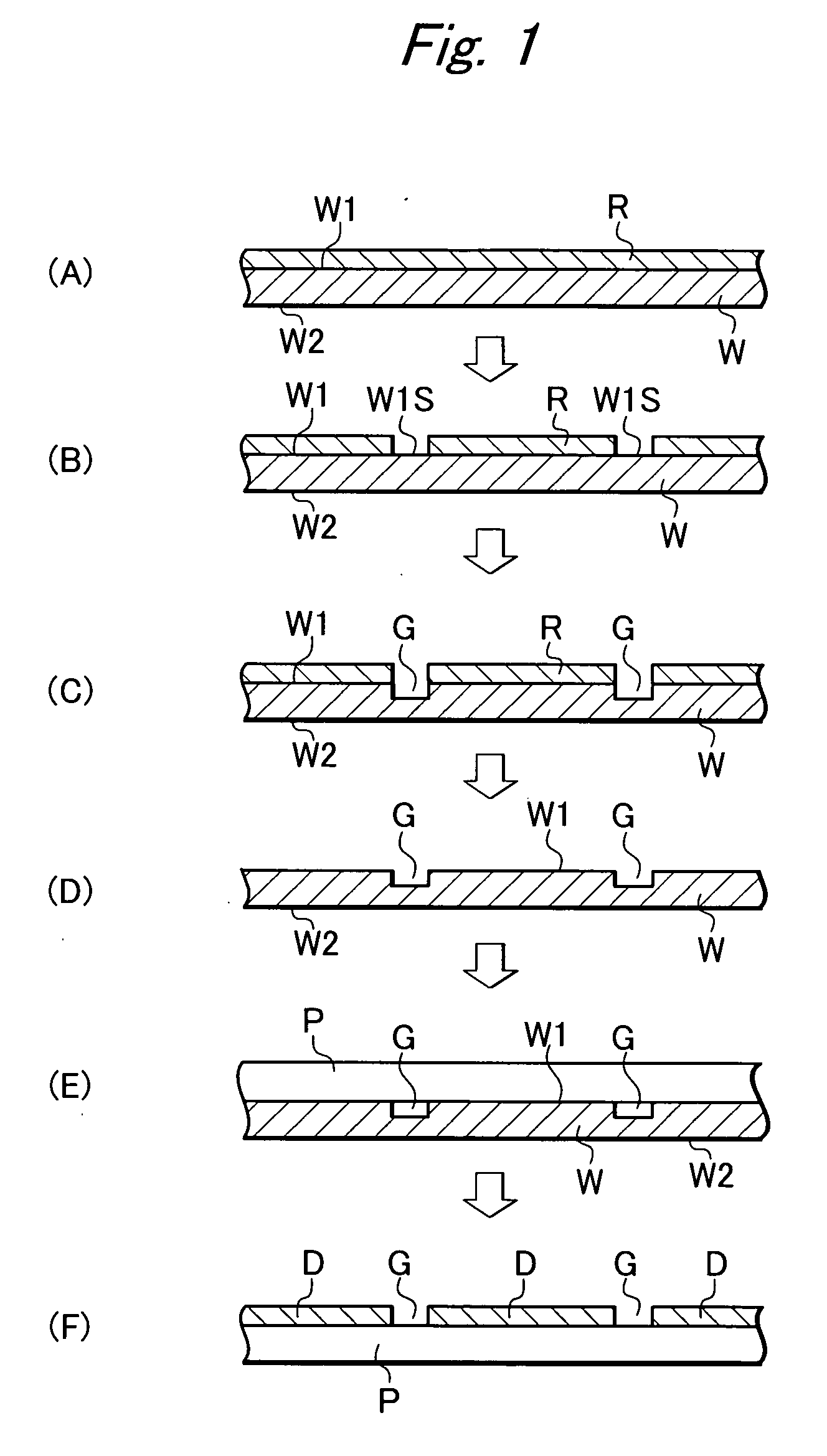
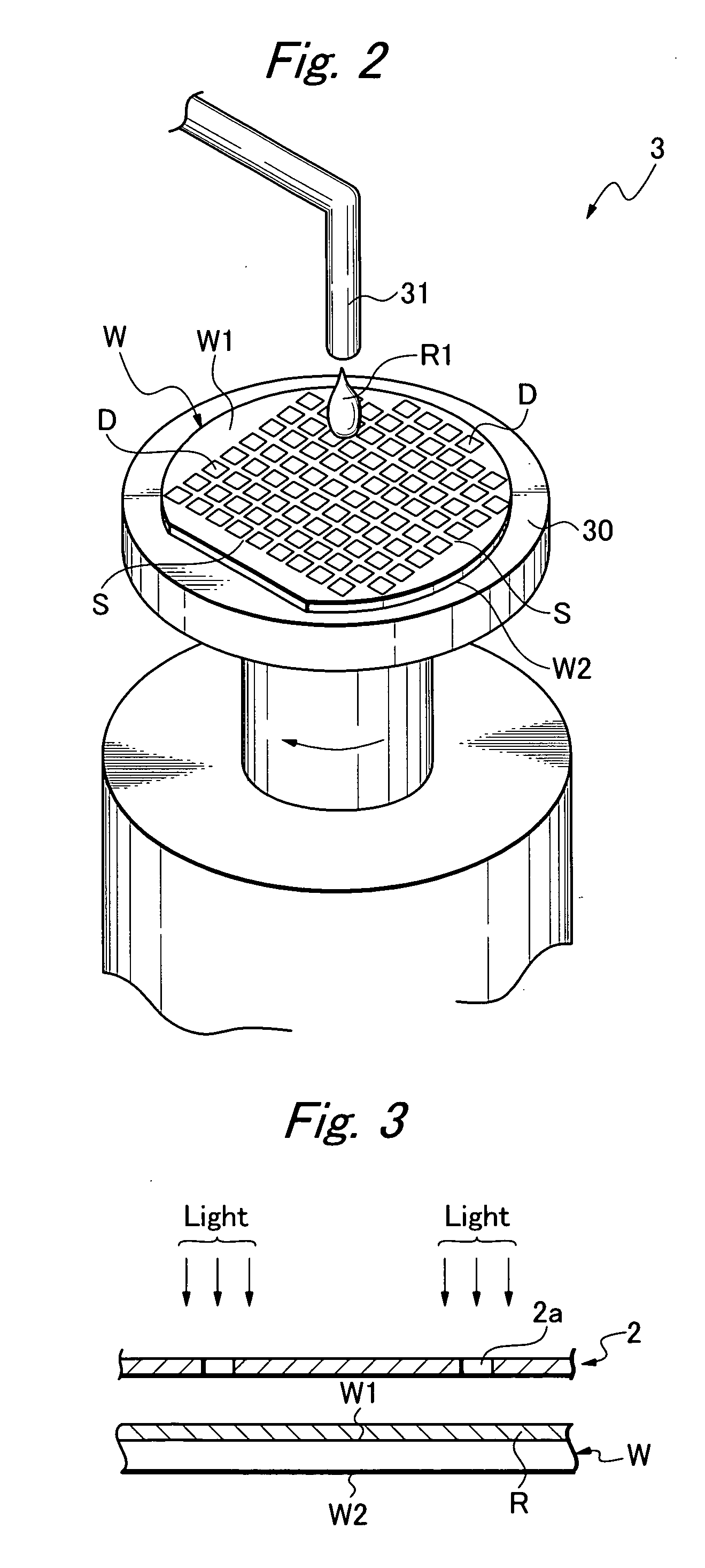
[0022] Referring to FIG. 1(A), first, the whole front surface W1 of a wafer W is coated with a resist film R. On the front surface W1 of the wafer W as shown in FIG. 2, there are formed a plurality of devices D being sectionalized by streets S. A spin coater 3 shown in FIG. 2, for example, can be used for coating the whole front surface W1 of the wafer W with the resist film R. In the spin coater 3 of FIG. 2, a back surface W2 of the wafer W is held by a holding table 30. A resist material R1 is dripped from a nozzle 31 while rotating the holding table 30, whereby the whole front surface W1 of the wafer W is coated with the resist film R as shown in FIG. 1(A).

[0023] Next, the front surface W1 of the wafer W is picked up the image by using a camera to recognize the streets S. Referring to FIG. 3, the resist film R is irradiated with light such as ultraviolet ray or X-ray via a photomask 2 having a mask pattern 2a formed like the same lattice as the streets S, so that portions of the...


PUM


Abstract

In order to efficiently divide the wafer into individual devices in dicing the wafer without deteriorating the quality of the devices, the front surface of the wafer is coated with a resist film except the regions corresponding to the streets, grooves of a depth corresponding to the finished thickness of the devices are formed by plasma etching in the regions corresponding to the streets, and the back surface of the wafer is ground so that the grooves are exposed from the side of the back surface and that the wafer is divided into individual devices.

Description

BACKGROUND OF THE INVENTION [0001] 1. Field of the Invention [0002] The present invention relates to a method of dividing a wafer. [0003] 2. Related Art [0004] A wafer having a plurality of devices formed on the front surface side thereof by being sectionalized by streets, is ground on its back surface to possess a predetermined thickness and is, then, cut and diced along the streets so as to be divided into individual devices and used in various electronic devices (see, for example, JP-A-2004228133). [0005] At the time of dicing, however, the cutting blade rotating at a high speed bites into the street of the wafer whereby the devices are partly cut away due to the crushing force of the cutting blade and, hence, the die strength of the devices constituting the wafer decreases to deteriorate the quality. [0006] At the time of dicing, further, the cutting blade is precisely positioned on each street to cut the streets one by one, which is not efficient. In particular, when the size o...

Claims


Application Information

Patent Timeline
IPC IPC(8): H01L21/78H01L21/302
CPCH01L21/304H01L21/3065H01L21/31138H01L21/67092H01L21/67132H01L21/78
Inventor FUJISAWA, SHINICHIMATSUHASHI, RYOUONO, TAKASHIFUNANAKA, TOSHIHIROHACHIYA, JUNKAWAI, AKIHITO
Owner DISCO CORP
Why Eureka
Try Eureka