Strain-engineered ferroelectric thin films

a thin film, ferroelectric technology, applied in the field of thin film structures, can solve the problems of degrading film properties and complicating their introduction into semiconductor fabrication facilities, and achieve the effects of enhancing the properties of ferroelectric materials, reducing the number of defects, and increasing the number of defects

Active Publication Date: 2006-05-04
PENN STATE RES FOUND +1
View PDF5 Cites 18 Cited by
  • Summary
  • Abstract
  • Description
  • Claims
  • Application Information

AI Technical Summary

Benefits of technology

[0004] In accordance with the present invention, the properties of ferroelectric materials are enhanced using appropriate control of the strain in thin films of such material for use in various applications including ferroelectric memories and electro-optical modulators. The thin films of ferroelectrics can have relatively non-volatile and non-toxic constituents which are well suited for semiconductor fabrication facilities and which are compatible with existing processing of silicon based devices. By control of the strain in the ferroelectric thin films in accordance with the present invention, much higher ferroelectric transition temperatures and much greater remanent polarizations can be achieved as compared to bulk single crystals of the same materials.

Problems solved by technology

Such strain may be undesirable and lead to degraded film properties, but in appropriate cases and at appropriate strain levels, the strain in the thin film can actually enhance the properties of the thin film for use in certain applications.
The major disadvantages in the use of these two materials are the volatility of the lead and bismuth constituents of these materials, which complicates their introduction into semiconductor fabrication facilities, and environmental issues associated with the toxicity of lead.

Method used


Image

  • Strain-engineered ferroelectric thin films
  • Strain-engineered ferroelectric thin films
  • Strain-engineered ferroelectric thin films

Examples


Embodiment Construction

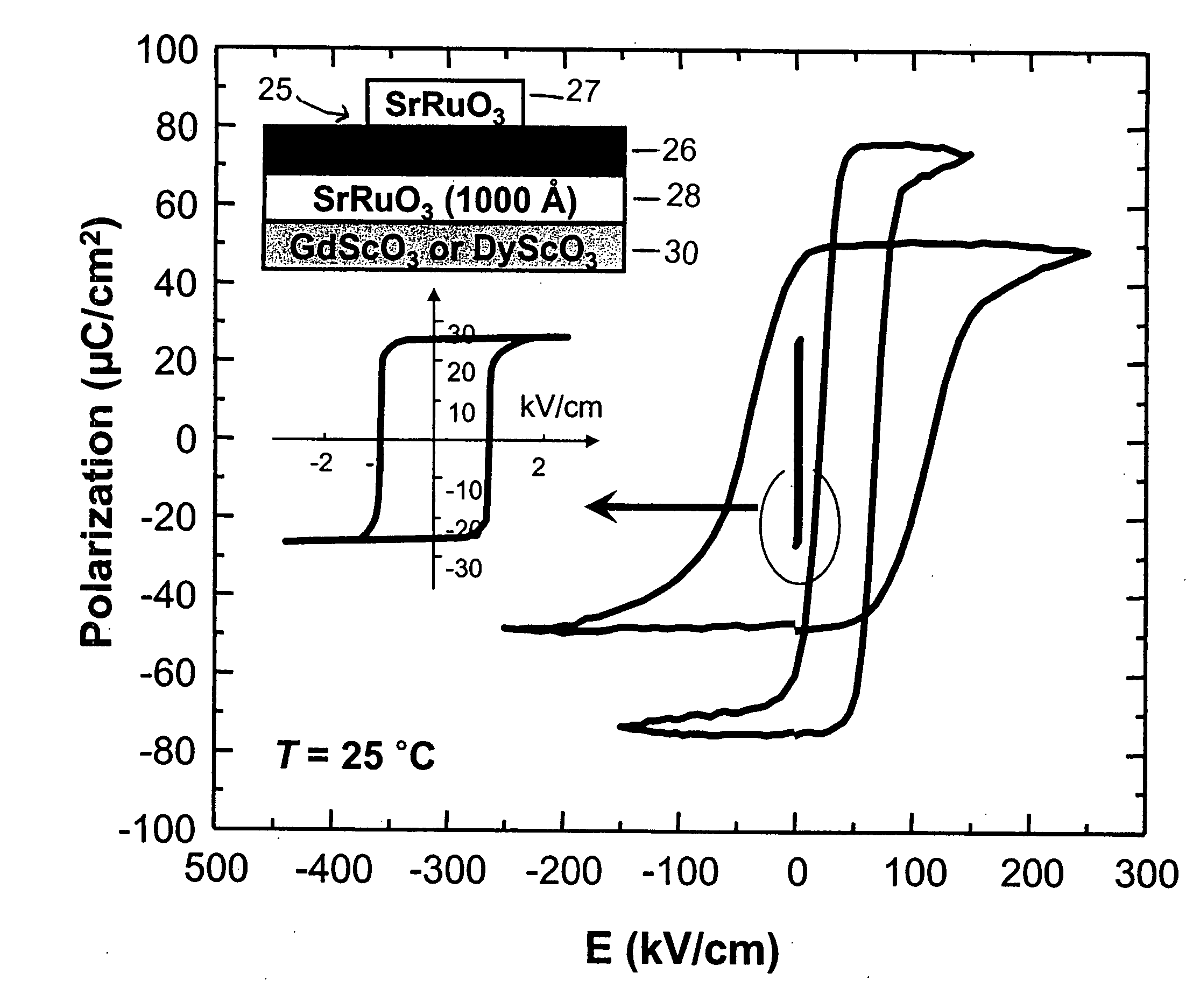
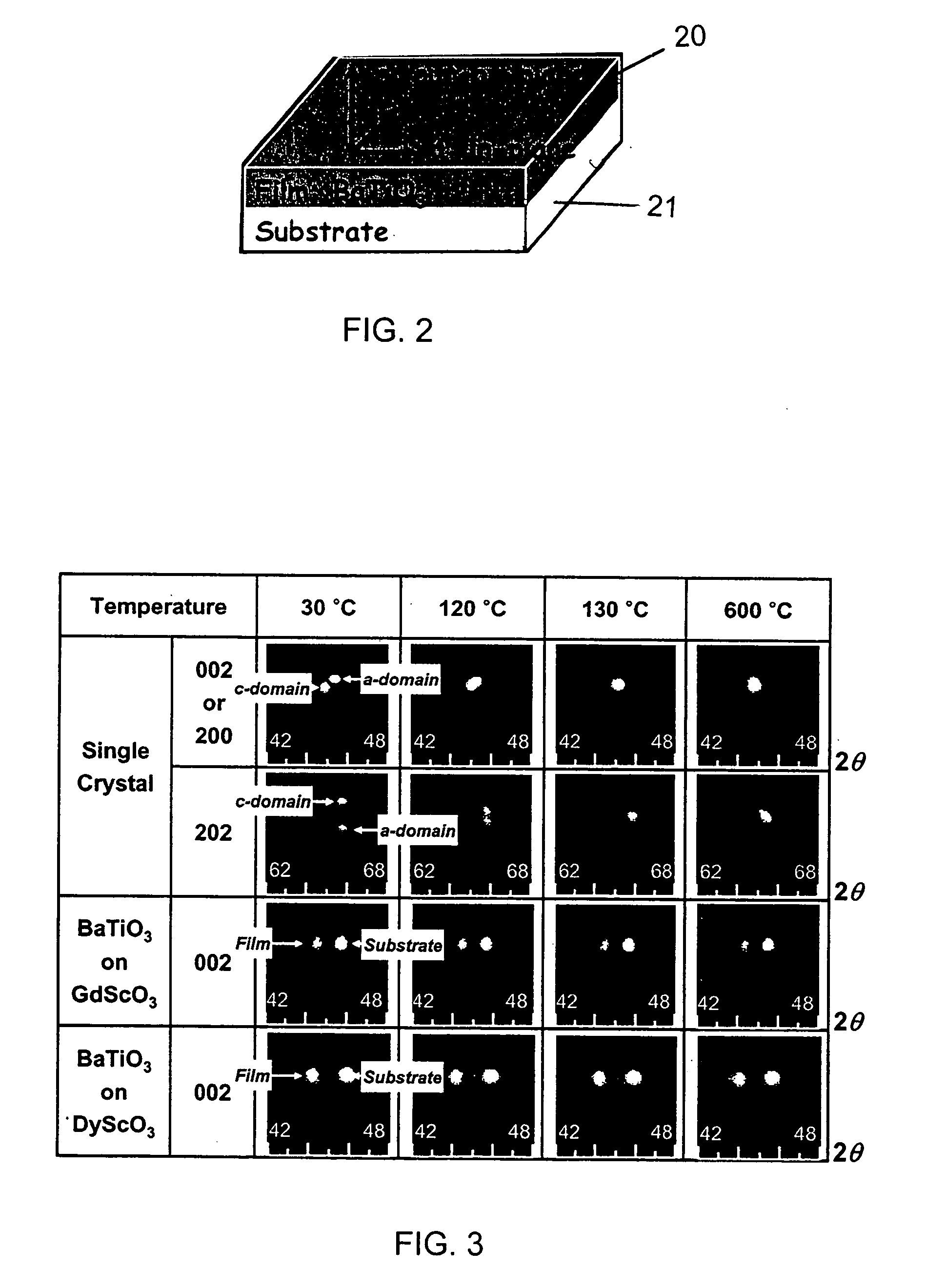
[0023] The present invention utilizes detailed investigations of the properties of ferroelectric thin films to achieve significantly improved ferroelectric properties as compared to the bulk ferroelectric. The present invention may be used with various crystalline ferroelectrics, examples only of which are BaTiO3, lead zirconium titanate (PZT), BiFeO3, and lead magnesium niobate-lead titanate (PMN-PT). For purposes of illustration, the invention is exemplified below with respect to BaTiO3, a preferred ferroelectric material, but it is understood that the invention is not limited thereto.

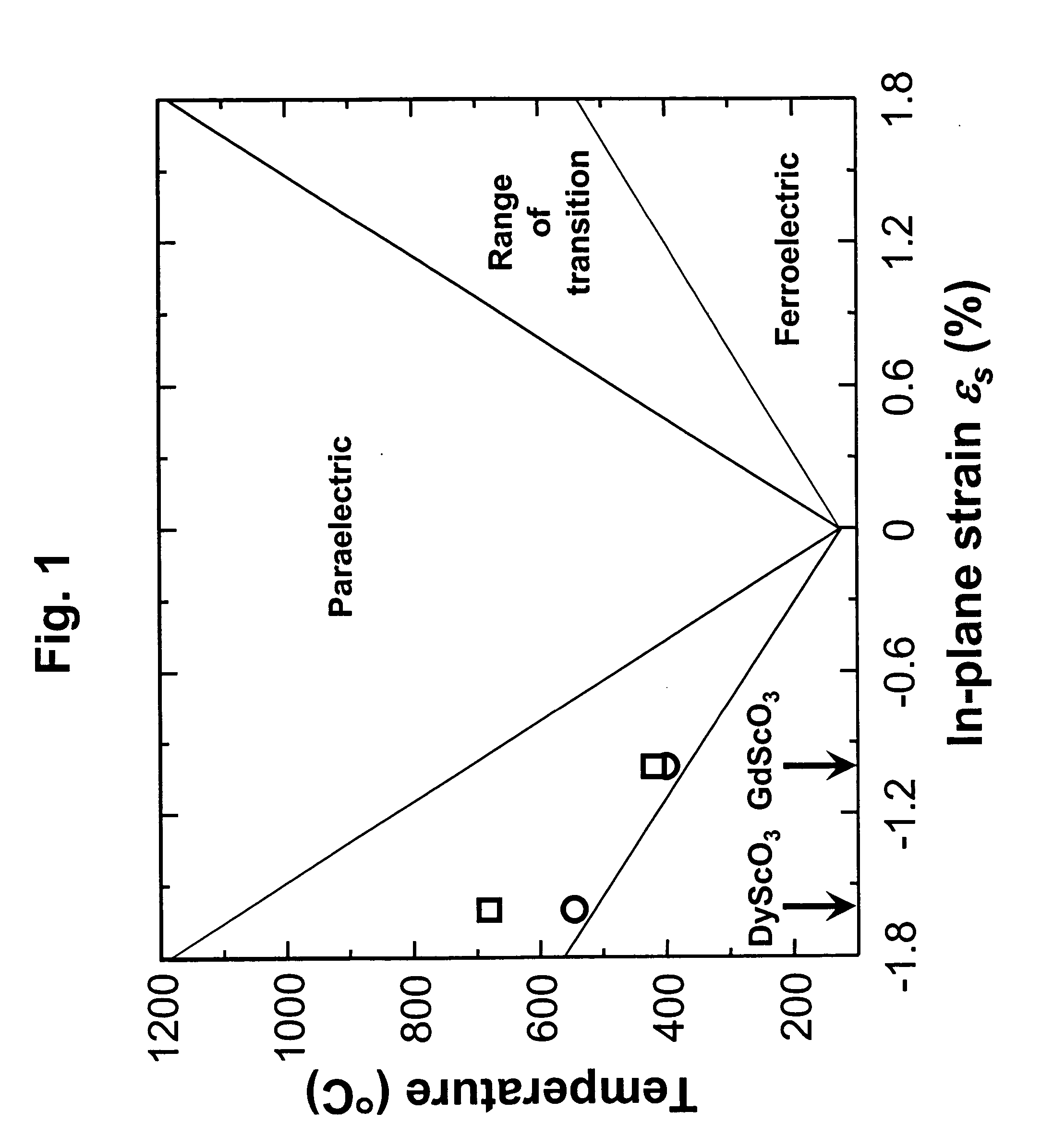
[0024] To predict the TC enhancement and the temperature dependence of the lattice parameters of BaTiO3 thin films under large biaxial strains using Landau thermodynamic theories, we determined a new set of phenomenological coefficients, since existing ones are only applicable to small compressive strains (C enhancement predicted from thermodynamic analysis for a BaTiO3 thin film under biaxial strai...


PUM

PropertyMeasurementUnit
thicknessaaaaaaaaaa
thicknessaaaaaaaaaa
thickaaaaaaaaaa

Abstract

A strained thin film structure includes a substrate layer formed of a crystalline scandate material having a top surface, and a strained layer of crystalline ferroelectric epitaxially grown with respect to the crystalline substrate layer so as to be in a strained state and at a thickness below which dislocations begin to occur in the crystalline ferroelectric layer. An intermediate layer may be grown between the top surface of the substrate layer and the ferroelectric layer wherein the intermediate layer carries the lattice structure of the underlying substrate layer. The properties of the ferroelectric film are greatly enhanced as compared to the bulk ferroelectric material, and such films are suitable for use in applications including ferroelectric memories.

Description

STATEMENT OF GOVERNMENT RIGHTS [0001] This invention was made with United States government support awarded by the following agency: NSF 0296021. The United States government has certain rights in this invention.FIELD OF THE INVENTION [0002] This invention pertains generally to the field of semiconductor and related device manufacturing and particularly to thin film structures. BACKGROUND OF THE INVENTION [0003] Very large strains can exist in thin films of one material deposited on another material due to differences in crystal lattice parameters and thermal expansion behavior between the thin film and the underlying substrate, or arising from defects formed during film deposition. As a result, the properties of such thin films can be dramatically different than the intrinsic properties of the corresponding unstrained bulk materials. Such strain may be undesirable and lead to degraded film properties, but in appropriate cases and at appropriate strain levels, the strain in the thin...

Claims


Application Information

Patent Timeline
Patent Type & Authority Applications(United States)
IPC IPC(8): H01L29/76
CPCH01L21/31691H01L29/516H01L21/02266H01L21/02197H01L21/02304
Inventor EOM, CHANG-BEOMCHOI, KYUNG-JINSCHLOM, DARRELL G.CHEN, LONG-QING
Owner PENN STATE RES FOUND
Why Eureka
Try Eureka