


Quick Research
Generate reliable direction feasibility study reports for your R&D in just a few steps.

Technical Q&A
Discover and master advanced knowledge NOW. Basics, ideas, possibilities, all at once.

Find Solutions
As an expert in R&D theories, this can generate solutions to your technical problems instantly.

Evaluate Feasibility
Analyze your overall solution with one click, know your potential R&D risks in advance.

Monitor Landscape
Get weekly tech updates, stay abreast of the latest tech innovations and key insights.
Bond pad structure for integrated circuit chip
a technology of integrated circuit chips and bond pads, which is applied in the direction of electrical equipment, semiconductor devices, semiconductor/solid-state device details, etc., can solve the problems of not allowing metal wiring circuitry and semiconductor devices to pass under or be located below the bond pad structure, and many low-k dielectric materials are highly susceptible to cracking or lack the strength needed to withstand some mechanical processes
- Summary
- Abstract
- Description
- Claims
- Application Information
AI Technical Summary
Benefits of technology
Problems solved by technology
Method used
Image

Examples
first embodiment
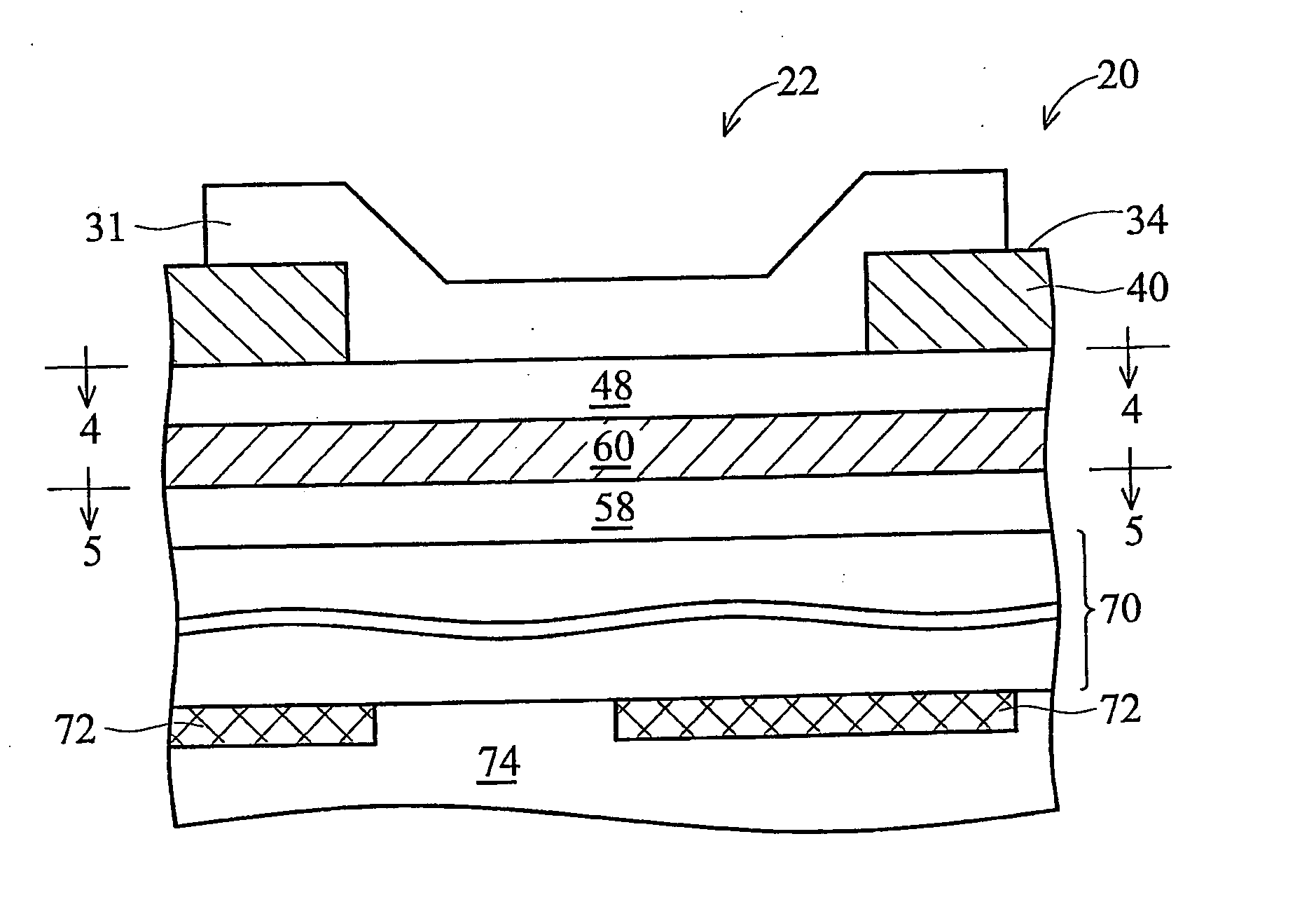
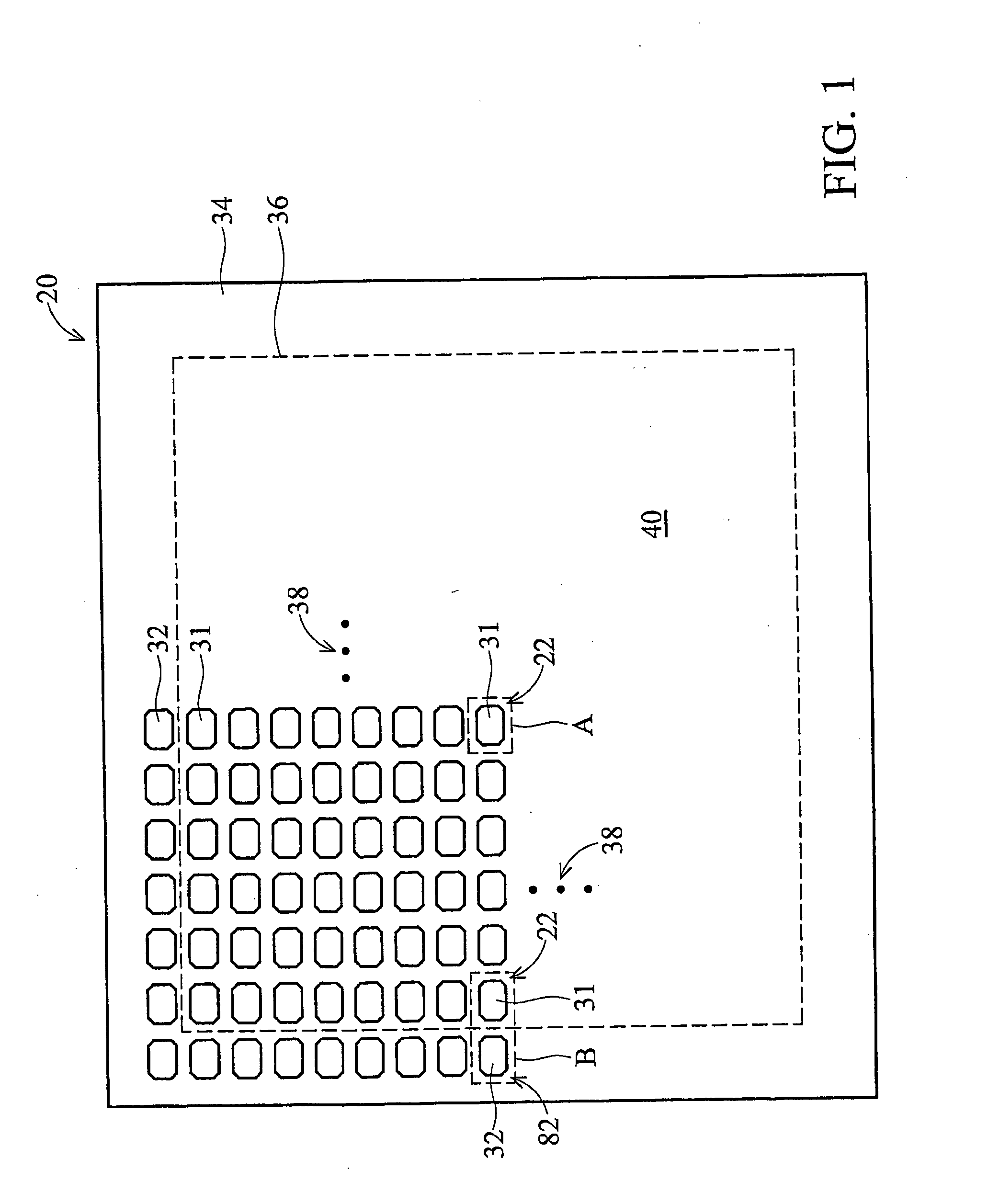
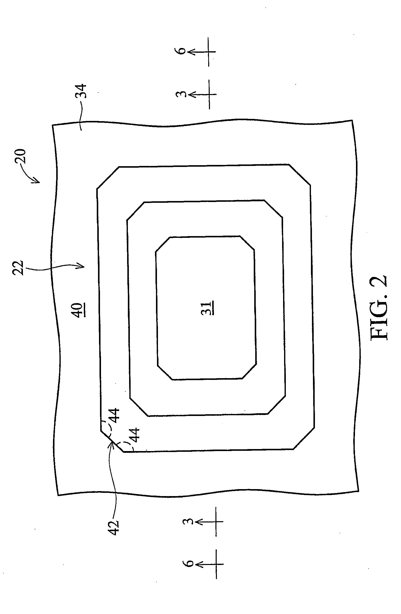
[0026] Referring now to FIGS. 1-5, various views of a first illustrative embodiment of the present invention are shown. More specifically, FIG. 1 is a top view of an integrated circuit chip 20 incorporating embodiments of the present invention. FIG. 2 is an enlarged view of portion A shown in FIG. 1. FIG. 3 is a cross-section view of a bond pad structure 22 of the first embodiment, as taken along line 3-3 in FIG. 2. FIG. 4 is a top sectional view showing an Mtop metal level of the bond pad structure 22, as taken along line 4-4 in FIG. 3. FIG. 5 is another top sectional view showing an Mtop−1 metal level of the bond pad structure 22, as taken along line 5-5 in FIG. 3.
[0027] Although FIG. 1 is referred to as a top view of the chip 20 herein showing the bond pads 31, 32 on the top surface 34 of the chip 20, the chip 20 may be operably mounted on a substrate (not shown) with the top surface 34 facing downward (e.g., flip chip bonding configuration). Hence, the term “top” is used herein ...
second embodiment
[0038]FIG. 7 is a top sectional view showing the conductive vias 78 located between the Mtop plate 48 and the Mtop−1 plate 58, as taken along line 7-7 in FIG. 6. The conductive vias 78 may be formed from any of a variety of suitable conductive materials, including (but not limited to): aluminum, gold, silver, nickel, copper, tungsten, titanium, tantalum, compounds thereof, alloys thereof, multiple layers thereof, composites thereof, and combinations thereof, for example. In a preferred embodiment, the Mtop plate 48 is electrically connected to the Mtop−1 plate 58 by the conductive vias 78. In other embodiments, however, the Mtop plate 48 may not be electrically connected to the Mtop−1 plate 58 by the conductive vias 78 (e.g., separated by a nonconductive layer or portion). In a preferred embodiment, at least some of the conductive vias 78 have a width of less than about 1 μm, for example. In the second embodiment, the Mtop−1 plate 58 is only electrically connected to the Mtop plate ...
third embodiment
[0039] Referring now to FIGS. 1 and 8-11, various views of a third illustrative embodiment of the present invention are shown. More specifically, FIG. 8 is an enlarged view of portion B shown in FIG. 1. FIG. 9 is a cross-section view of two different bond pad structures 22, 82 of the third embodiment, as taken along line 9-9 in FIG. 8. FIG. 10 is a top sectional view showing an Mtop metal level of the two bond pad structures 22, 82, as taken along line 10-10 in FIG. 9. FIG. 11 is another top sectional view showing an Mtop−1 metal level of the two bond pad structures 22, 82, as taken along line 11-11 in FIG. 9.
[0040] The third embodiment focuses on an integrated chip 20 having a first bond pad structure 22 with at least part of at least one active circuit 72 located there under, and a second bond pad structure 82 with no active circuit there under. In some embodiments of the present invention (not shown), all of the bond pad structures may be located over the active circuit area. As ...
PUM
 Abstract
Description
Claims
Application Information
 - R&D Engineer
- R&D Manager
- IP Professional
- Industry Leading Data Capabilities
- Powerful AI technology
- Patent DNA Extraction
Browse by: Latest US Patents, China's latest patents, Technical Efficacy Thesaurus, Application Domain, Technology Topic, Popular Technical Reports.
© 2024 PatSnap. All rights reserved.Legal|Privacy policy|Modern Slavery Act Transparency Statement|Sitemap|About US| Contact US: help@patsnap.com