Structure having a characteristic of conducting or absorbing electromagnetic waves
a technology of electromagnetic waves and structures, applied in the field of structures having a characteristic of conducting or absorbing electromagnetic waves, can solve the problems of high cost, difficult steps, and difficulty in regularly aligning particles, and achieve the effect of easy production and low cos
- Summary
- Abstract
- Description
- Claims
- Application Information
AI Technical Summary
Benefits of technology
Problems solved by technology
Method used
Image
Examples
example 1
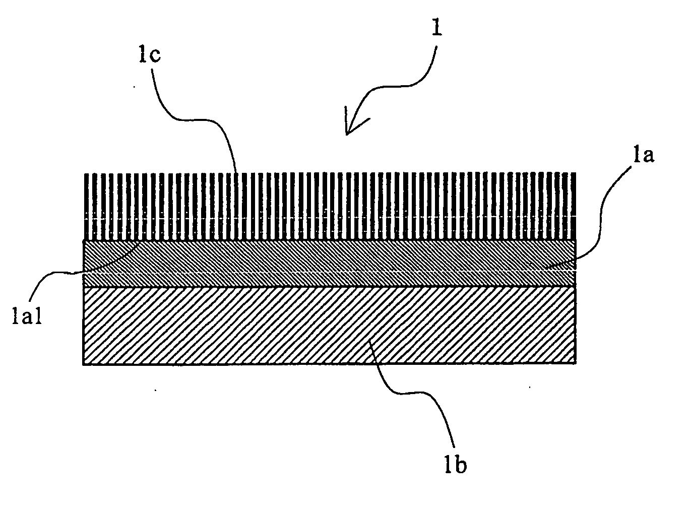
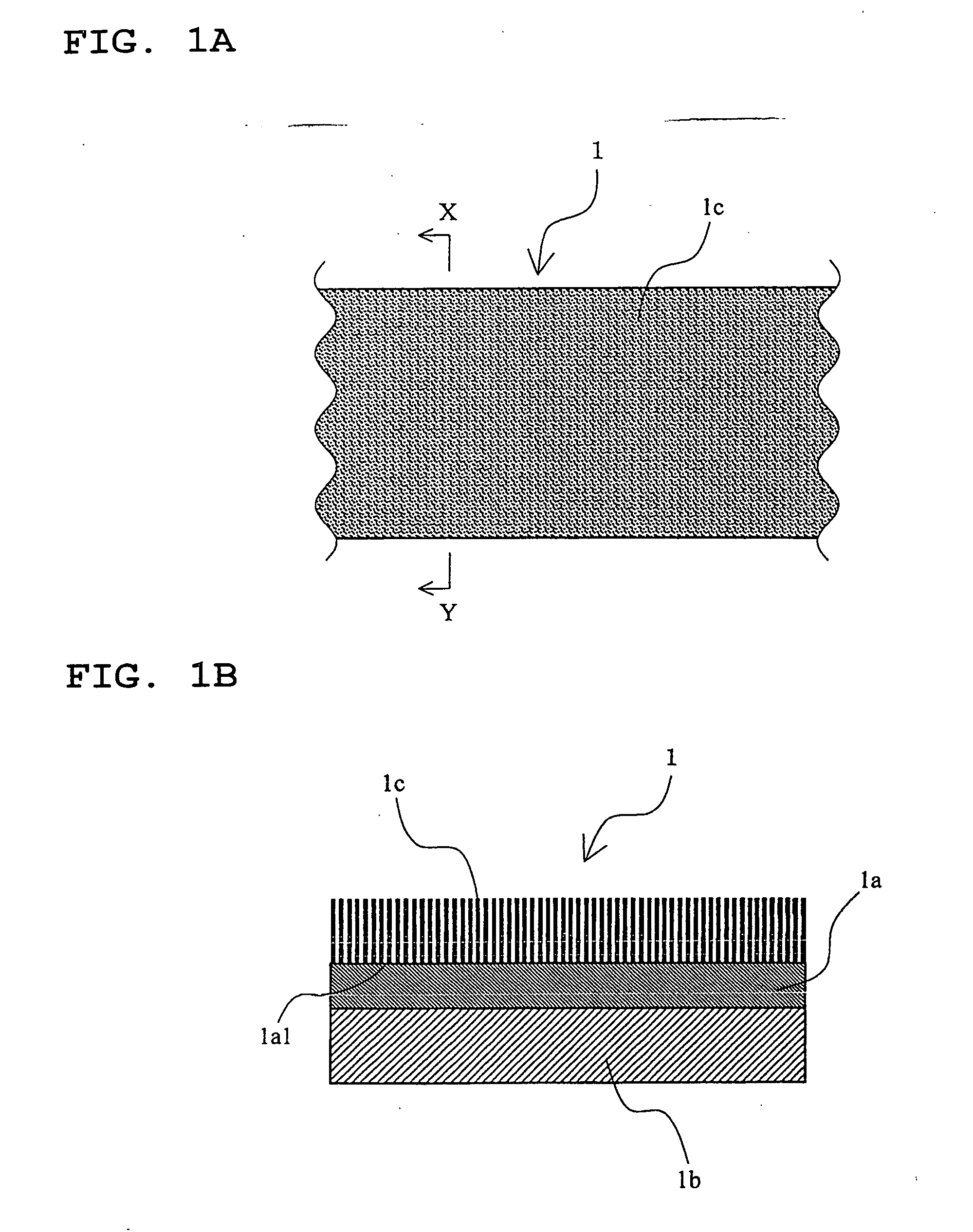
[0216] On one surface of an aluminum-made base material (thickness: 10 μm) as an electromagnetic conducting or absorbing base material, an acrylic pressure-sensitive adhesive (base polymer: butyl acrylate / acrylic acid copolymer) having 35% by weight (proportion based on the whole amount of solids) of a nickel powder blended therein was coated in a thickness after drying of 30 μm to form an electromagnetic conducting or absorbing pressure-sensitive adhesive layer. Thereafter, the entire surface of the subject electromagnetic conducting or absorbing pressure-sensitive adhesive layer was subjected to electrostatic flocking processing by using, as an electromagnetic conducting or absorbing fiber, an acrylic fiber whose surface had been subjected to a nickel plating treatment (a plating treatment with nickel) (fiber thickness: 3 deniers, fiber length: 0.5 mm), thereby flocking the foregoing acrylic fiber whose surface had been subjected to a nickel plating treatment on the entire surface...
example 2
[0218] The same procedures as in Example 1 were followed, except for using, as the electromagnetic conducting or absorbing fiber, an acrylic fiber (fiber thickness: 3 deniers, fiber length: 0.5 mm) whose surface had been subjected to a copper-nickel plating treatment (a plating treatment with a copper-nickel alloy), thereby preparing a sheet-like structure (hereinafter sometimes referred to as “sheet-like structure A2”) in a form that an electromagnetic conducting or absorbing fiber napping section (a fiber napping section composed of an acrylic fiber whose surface had been subjected to a copper-nickel plating treatment) was formed entirely on the surface of the electromagnetic conducting or absorbing pressure-sensitive adhesive layer formed on the electromagnetic conducting or absorbing base material.
example 3
[0219] The same procedures as in Example 1 were followed, except for using, as the electromagnetic conducting or absorbing fiber, an acrylic fiber (fiber thickness: 3 deniers, fiber length: 0.5 mm) whose surface had been subjected to a copper plating treatment (a plating treatment with copper), thereby preparing a sheet-like structure (hereinafter sometimes referred to as “sheet-like structure A3”) in a form that an electromagnetic conducting or absorbing fiber napping section (a fiber napping section composed of an acrylic fiber whose surface had been subjected to a copper plating treatment) was formed entirely on the surface of the electromagnetic conducting or absorbing pressure-sensitive adhesive layer formed on the electromagnetic conducting or absorbing base material.
PUM
| Property | Measurement | Unit |
|---|---|---|
| Fraction | aaaaa | aaaaa |
| Frequency | aaaaa | aaaaa |
| Frequency | aaaaa | aaaaa |
Abstract
Description
Claims
Application Information


