Thermal enhance package and manufacturing method thereof

Inactive Publication Date: 2006-05-04
ADVANCED SEMICON ENG INC
View PDF9 Cites 9 Cited by
  • Summary
  • Abstract
  • Description
  • Claims
  • Application Information

AI Technical Summary

Benefits of technology

[0012] As mentioned above, the pellets connect the heat spreader units and the substrate units so as to upgrade the thermal perfo

Problems solved by technology

Integrated circuit (chip) packaging technology is becoming a limiting factor for the development in packaged integrated circuits of higher performance.
Semiconductor package designers are struggling to keep pace with the increase in pin count, size limitations, low profile, and other evolving

Method used


Image

  • Thermal enhance package and manufacturing method thereof
  • Thermal enhance package and manufacturing method thereof
  • Thermal enhance package and manufacturing method thereof

Examples


Example

[0023] The thermal enhance package and a manufacturing method thereof according to the preferred embodiment of this invention will be described herein below with reference to the accompanying drawings, wherein the same reference numbers refer to the same elements.

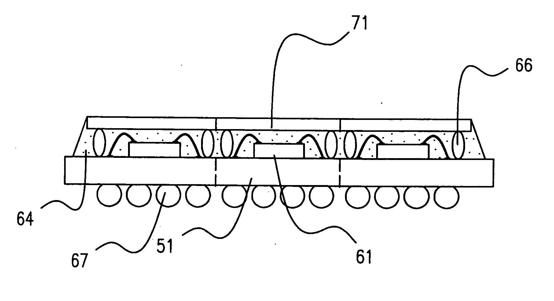
[0024] In accordance with a first preferred embodiment as shown in FIG. 7A, the thermal enhance package mainly comprises a substrate unit 51, a chip 61, a plurality of conductive wires 63, an encapsulation unit 64, a heat spreader unit 71 and a plurality of pellets 66. The substrate unit 51 has an upper surface 512 and a lower surface 514, and the chip 61 is disposed on the upper surface 512 of the substrate unit 51 and electrically connected to the substrate unit 51. Furthermore, the heat spreader unit 71 is disposed above the chip 61, and the pellets 66 are disposed on the upper surface 512 of the substrate unit 51 and connected to the heat spreader unit 71. And an encapsulation unit 64 encapsulates at least the pellets ...


PUM


Abstract

A thermal enhance package mainly comprises a chip, a substrate unit, a heat spreader unit and a plurality of pellets. The chip is disposed above the substrate unit and electrically connected to the substrate unit, and an encapsulation unit encapsulates the chip, the substrate unit, the heat spreader unit and the pellets. Therein the pellets are formed on the substrate unit and connect the substrate unit and the heat spreader unit. Thus the heat arisen out of the chip can be transmitted to the heat spreader unit not only through the encapsulation unit but also the pellets. Moreover, the substrate unit has at least one grounding contact connecting to one of the pellets so as to provide the thermal enhance package a good shielding. In addition, a method for manufacturing the thermal enhance package is also provided.

Description

BACKGROUND OF THE INVENTION [0001] 1. Field of Invention [0002] This invention relates to a thermal enhance package. More particularly, the present invention is related to a thermal enhance ball grid array package and a manufacturing method thereof. [0003] 2. Related Art [0004] Integrated circuit (chip) packaging technology is becoming a limiting factor for the development in packaged integrated circuits of higher performance. Semiconductor package designers are struggling to keep pace with the increase in pin count, size limitations, low profile, and other evolving requirements for packaging and mounting integrated circuits. Nowadays, ball grid array package (BGA) and chip scale package (CSP) are wildly applied to chip package with high I / Os and assembly package for thermal enhance integrated circuits. [0005] Originally, as shown in FIGS. 1, 2 and 3, a conventional manufacturing method of ball grid array package comprises the following steps. First, referring to FIG. 1, a substrate...

Claims


Application Information

Patent Timeline
IPC IPC(8): H01L21/50H01L21/48H01L21/56H01L23/31H01L23/36H01L23/433H01L23/552
CPCH01L21/4882H01L2224/48247H01L21/565H01L23/16H01L23/3128H01L23/36H01L23/4334H01L23/49816H01L23/552H01L24/17H01L24/97H01L2224/13099H01L2224/16225H01L2224/48091H01L2224/48227H01L2224/97H01L2924/01047H01L2924/01079H01L2924/01082H01L2924/14H01L2924/15311H01L2924/16152H01L2924/3025H01L21/561H01L2224/16245H01L2224/45144H01L2924/014H01L2924/01076H01L2924/01033H01L2924/01024H01L24/48H01L2224/85H01L2924/00014H01L2224/81H01L2924/00H01L2924/12042H01L24/45H01L2924/181H01L2924/00015H01L2224/05599H01L2924/00012H01L2224/0401
Inventor TAO, SU
Owner ADVANCED SEMICON ENG INC
Why Eureka
Try Eureka