Method and apparatus for forming a thin-film solar cell using a continuous process

a technology of continuous process and thin film, applied in the field of photovoltaics, can solve the problems of insufficient reduction of product cost, difficult scaling into commercial scale processes, and efficient thin film manufacturing process, so as to prevent chemical cross-contamination, prevent cross-contamination, and optimize recovery

Inactive Publication Date: 2006-05-11
DAYSTAR TECHNOLOGIES
View PDF18 Cites 141 Cited by
  • Summary
  • Abstract
  • Description
  • Claims
  • Application Information

AI Technical Summary

Benefits of technology

[0010] It is also understood that additional zones may be employed to isolate deposition or treatment zones from one another to prevent chemical cross-contamination and to allow optimal recovery. These isolation zones can range in the duration the work piece resides therein in order to allow the exposed substrate to reach an optimal condition for the next production step in a vacuum seal to prevent cross-contamination.

Problems solved by technology

Unfortunately, product costs have not been sufficiently reduced to open up the critical markets in the developing world where electricity demand is driving them to polluting, non-renewable sources such as coal and oil.
However, although relatively efficient PV cells can be manufactured in the laboratory, it has proven difficult to scale into commercial scale processes with consistent repeatability and efficiency critical for commercial viability.
The lack of an efficient thin-film manufacturing process has contributed to the failure of PV cells to effectively replace alternate energy sources in the market.
Currently, cells are manufactured using a multi-step batch process wherein each product piece is transferred between reaction steps and such transfer is bulky and requires reaction in chambers to be cycled.
One drawback to this process is that the substrate is transferred from vacuum to air and back to vacuum several times. An alternate system uses a series of individual batch processing chambers coupled with a roll-to-roll continuous process for each chamber.
The major drawback in this process is the discontinuity of the system and the need to break vacuum.
Using approaches as outlined above, one or more defects can render the entire plate (a single device) useless and result in zero yield for that unit of product.
These and other problems have relegated thin-film technologies to less than 10% market share worldwide.

Method used


Image

  • Method and apparatus for forming a thin-film solar cell using a continuous process
  • Method and apparatus for forming a thin-film solar cell using a continuous process
  • Method and apparatus for forming a thin-film solar cell using a continuous process

Examples


Embodiment Construction

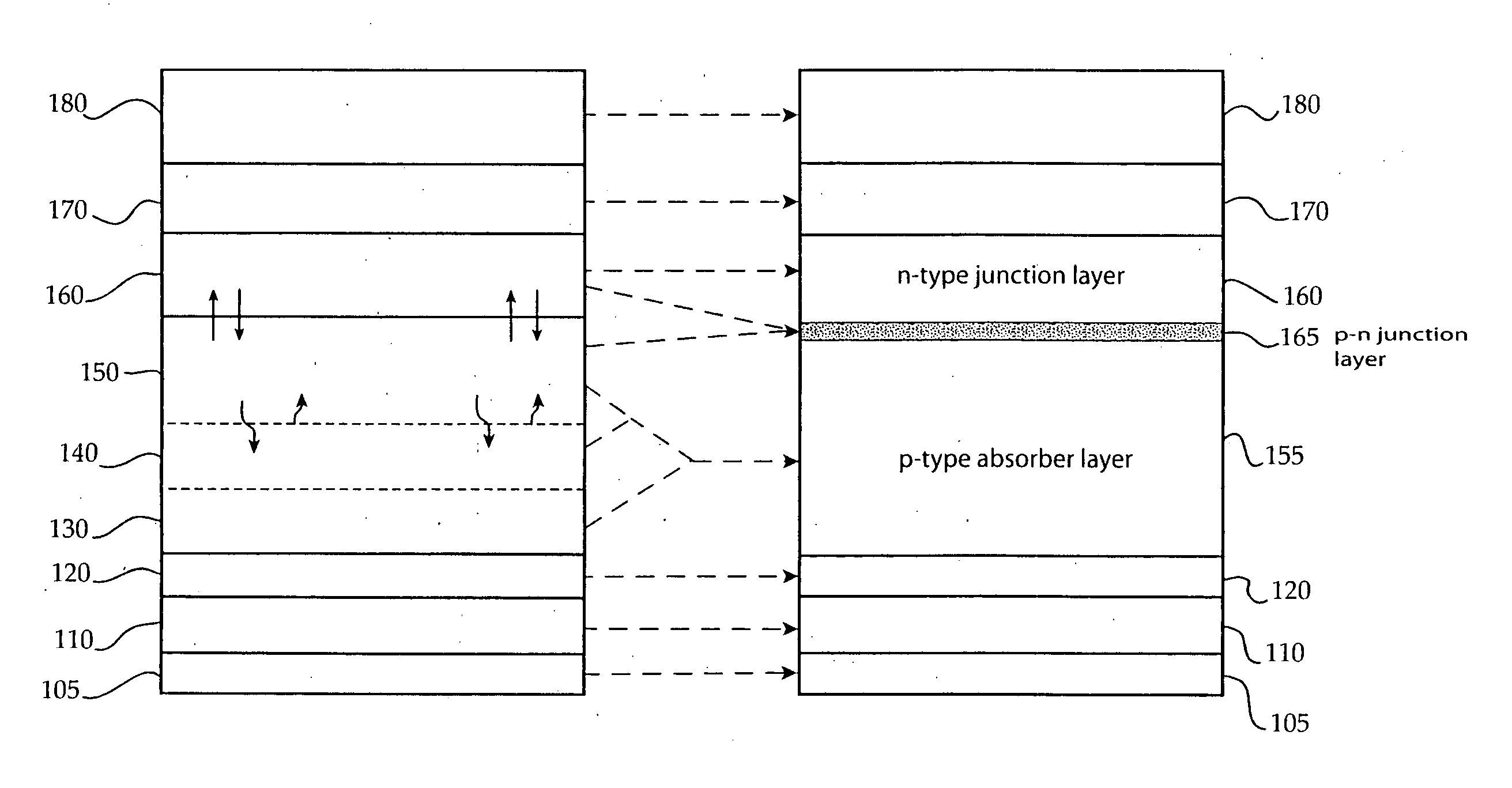
[0021] The present invention employs a new production apparatus in order to produce photovoltaic devices. The particular apparatus will depend upon the specific photovoltaic device design, which can be varied. FIG. 1 shows a photovoltaic device or thin-film solar cell 100 comprising a substrate 105, a barrier layer 110, a back contact layer 120, a semiconductor layer 130, alkali materials 140, another semiconductor layer 150, an n-type junction buffer layer 160, an intrinsic transparent oxide layer 170, and a transparent conducting oxide layer 180. It will be recognized by one skilled in the art that the thin film solar cell may comprise fewer layers and still function according to the invention. For instance, the device need not have alkali-materials.

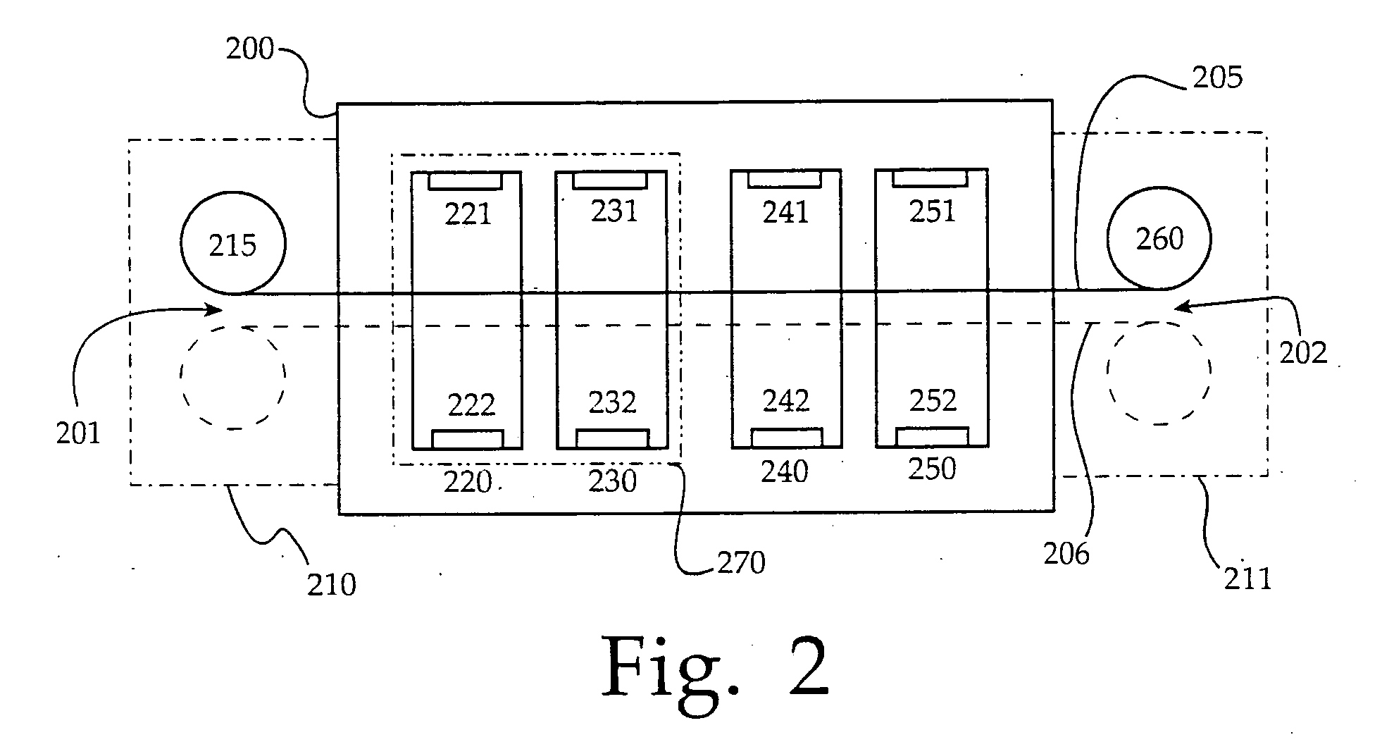
[0022] Two variations of an integrated production apparatus are provided. In each case, a series of treatment chambers are provided, where each chamber provides a specific treatment regimen in order to produce a specific layer deposit...


PUM

PropertyMeasurementUnit
thicknessaaaaaaaaaa
temperatureaaaaaaaaaa
pressureaaaaaaaaaa

Abstract

The present invention relates to new methods for manufacturing photovoltaic devices and an apparatus for practicing those methods of manufacture. The present invention employs a transfer-through system for advancing work piece substrates through an integrated apparatus of multiple treatment chambers that control each of the manufacturing processes.

Description

CROSS-REFERENCE TO RELATED APPLICATIONS [0001] This application claims priority from U.S. Provisional Patent Application Ser. No. 60 / 626,843, filed Nov. 10, 2004.BACKGROUND OF THE INVENTION [0002] The invention disclosed herein relates generally to the field of photovoltaics and more specifically to manufacturing thin-film solar cells using a continuous process and thin film solar cells made according to the process. DESCRIPTION OF THE RELATED ART [0003] Photovoltaic (PV) cells, modules and power systems offer clean, reliable, renewable energy to the world's expanding demand for electrical power. Unfortunately, product costs have not been sufficiently reduced to open up the critical markets in the developing world where electricity demand is driving them to polluting, non-renewable sources such as coal and oil. With the population expanding, and per-capita energy consumption going up, the world is heading towards an irreconcilable future where energy demand and supply irreversibly d...

Claims


Application Information

Patent Timeline
Patent Type & Authority Applications(United States)
IPC IPC(8): C23C16/00
CPCC23C14/562C23C14/568H01L31/0322H01L31/03928H01L31/0749H01L31/1876Y02E10/541Y02P70/50
Inventor TUTTLE, JOHN R.
Owner DAYSTAR TECHNOLOGIES
Why Eureka
Try Eureka