Low-k dielectric layer formed from aluminosilicate precursors

a technology of aluminosilicate and precursors, which is applied in the direction of coatings, basic electric elements, chemical vapor deposition coatings, etc., can solve the problems of reducing the density and mechanical strength of ild materials, reducing the resistance of copper metals, and reducing the k-valu

Inactive Publication Date: 2006-05-11
INTEL CORP
View PDF13 Cites 15 Cited by
  • Summary
  • Abstract
  • Description
  • Claims
  • Application Information

AI Technical Summary

Problems solved by technology

However, copper has the lowest resistivity of metals that can easily be incorporated into IC devices, making reduction of ILD dielectric constant critical for realizing further decreases in interconnect delay times.
These techniques lower the k-value; however, they also reduce the density and mechanical strength of the ILD material.
As a result, these materials are easily damaged by stresses imparted to the ILD during subsequent IC device fabrication processing.
Damage could inclu

Method used


Image

  • Low-k dielectric layer formed from aluminosilicate precursors
  • Low-k dielectric layer formed from aluminosilicate precursors
  • Low-k dielectric layer formed from aluminosilicate precursors

Examples


Embodiment Construction

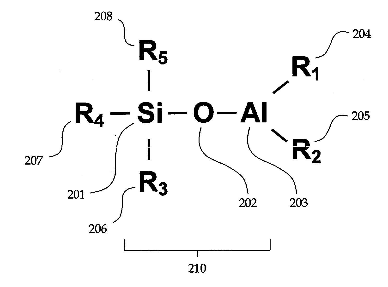
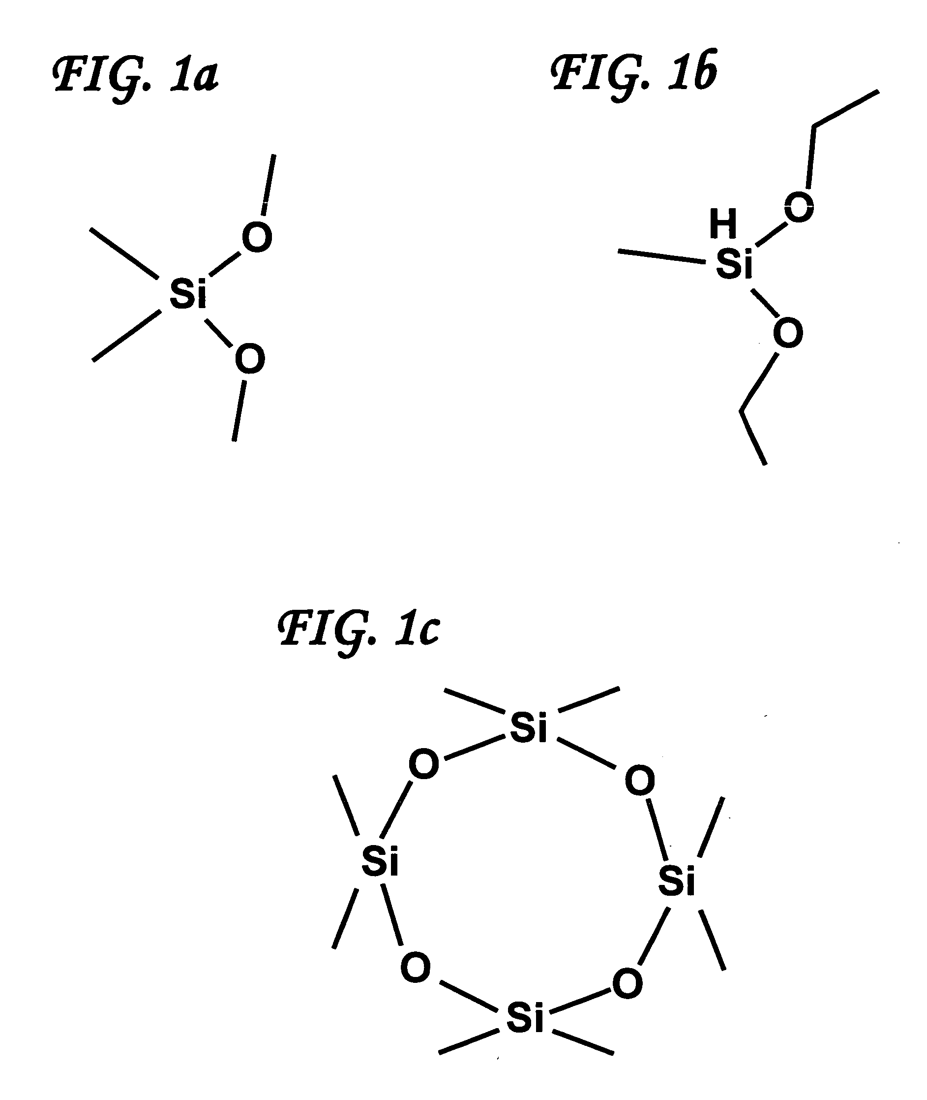
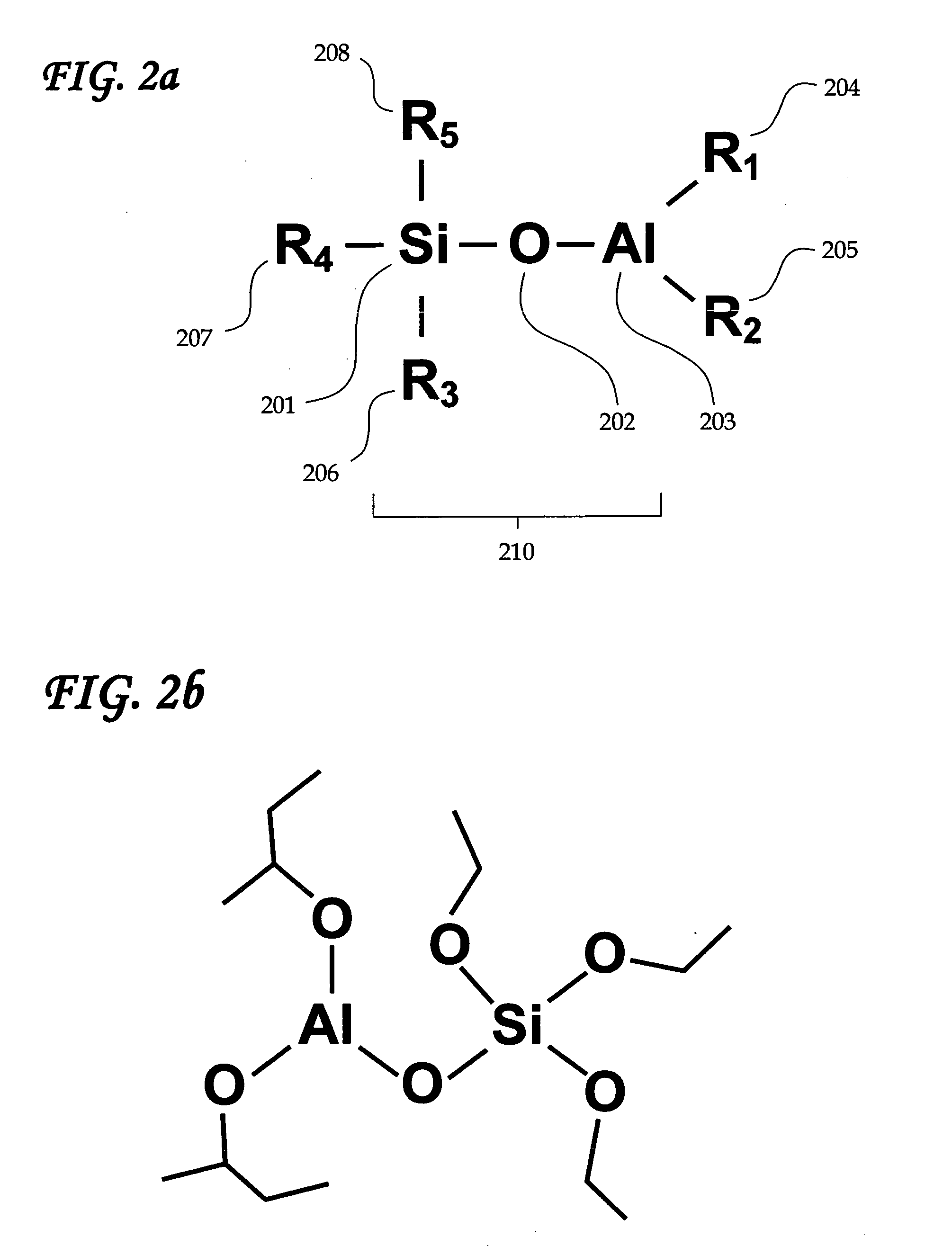
[0014] Disclosed are numerous embodiments of a thin film interlayer dielectric (ILD) material formed using a class of aluminum-bearing precursors referred to herein as ‘aluminosilicate’ precursors. In an embodiment, these precursors may provide a low-k dielectric material with higher mechanical strength (as characterized by elastic modulus, hardness, or cohesive strength) than is available via similar methods or materials using low-k silicon-based precursors not containing aluminum or other metal atoms (typical examples of which are shown in FIGS. 1a-1c). The increase in mechanical strength of the dielectric material formed in this embodiment may help to reduce the incidence of damage (e.g. cracking) incurred due to physically or thermally induced stresses to the integrated circuit device. These stresses are inherent to the manufacturing process and end use of IC devices in which the dielectric material is used.

[0015] Precursors generally are substances that precede some transition...


PUM

PropertyMeasurementUnit
Dielectric polarization enthalpyaaaaaaaaaa

Abstract

A method for forming a high mechanical strength, low k, interlayer dielectric material with aluminosilicate precursors so that aluminum is facilely incorporated into the silicon matrix of the material, and an integrated circuit device comprising one or more high-strength, low-k interlayer dielectric layers so formed.

Description

FIELD OF THE INVENTION [0001] The present invention relates generally to the field of semiconductor integrated circuit (IC) manufacturing. In particular, the present invention relates to a method for forming a low-k dielectric material in an integrated circuit device, and the material so formed. BACKGROUND OF THE INVENTION [0002] IC manufacturing typically involves the sequential formation of multiple layers to form a single integrated device. The materials for each layer are chosen either because their properties allow them to inherently meet the required performance criteria for the IC device, or because their properties can be altered through the manufacturing process so that they meet those criteria. One type of material used to form a layer within an IC device is a dielectric. [0003] Dielectric materials are electrical insulators, used to substantially electrically isolate conductive layers or features within the IC. The ratio of the amount of electrostatic energy that can be s...

Claims


Application Information

Patent Timeline
IPC IPC(8): H01L23/58H01L21/469
CPCC23C16/401H01L21/02145H01L21/02203H01L21/02216H01L21/02274H01L21/3122H01L21/76825H01L2924/0002H01L21/76828H01L21/76829H01L23/5329H01L2924/00
Inventor GOODNER, MICHAEL D.
Owner INTEL CORP
Why Eureka
Try Eureka