
Simultaneous planarization of pole piece and coil materials for write head applications

a write head and coil material technology, applied in the field of thin film heads, can solve the problems of difficult control of the geometry of the pb>2/b> photoresist mask, the difficulty of varying the ferromagnetic properties the difficulty of achieving uniform thickness of the pb>2/b> layer, etc., to achieve the effect of improving the equalization of copper, low surface energy and higher surface energy

Inactive Publication Date: 2006-05-11
HITACHI GLOBAL STORAGE TECH NETHERLANDS BV
View PDF20 Cites 1 Cited by
  • Summary
  • Abstract
  • Description
  • Claims
  • Application Information

AI Technical Summary

Benefits of technology

The patent describes a new method for planarizing surfaces using a special slurry that can remove materials with different rates of removal. This slurry is designed to work well with copper, hardbaked resist, alumina, and NiFe structures, which are commonly used in thin film magnetic head processes. The slurry contains an oxidant, a complexing agent, an abrasive, and a surfactant. The slurry is applied to the surface of the structures and then planarized using a chemical mechanical planarization technique. The method can improve the overall quality of the planarized surfaces.

Problems solved by technology

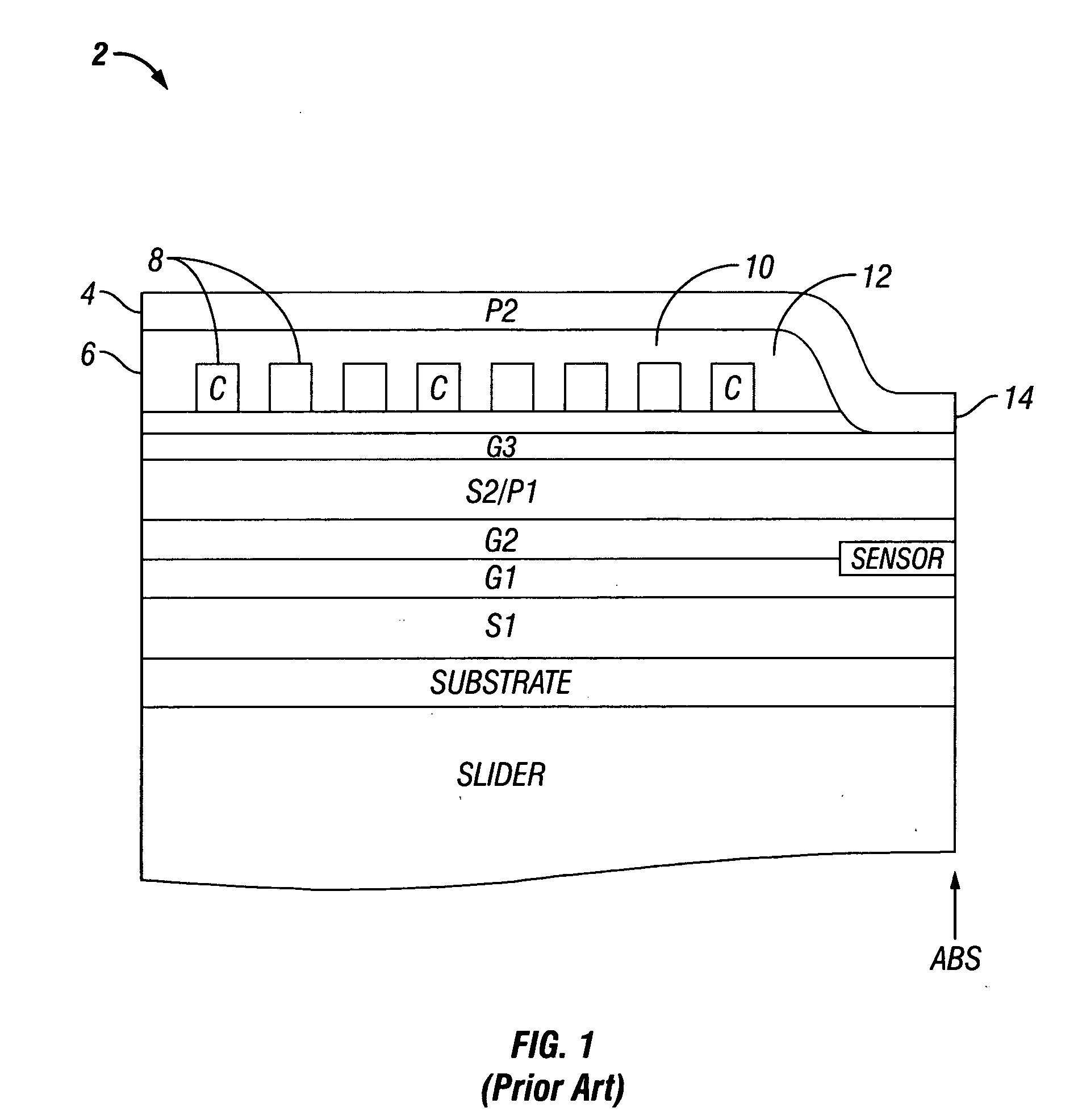
A disadvantage of this technique is that the ill-defined slope 12 of the integrated layer 6 as it approaches the pole tip 14 makes it difficult to control the geometry of the P2 photoresist mask.
In addition, the application of P2 material onto the integrated layer's sloped surface can produce a P2 layer having non-uniform thickness and varying ferromagnetic properties.
A further disadvantage is that write head track width is difficult to control.
Each of the foregoing problems may be present to different degrees in any given write head of a single fabrication batch, or between write heads produced in different fabrication batches.
This makes repeatability of results difficult to achieve and reduces production yields accordingly.
The difficulty with using CMP planarization for the improved write head application described above is that current CMP methods will not polish away the four involved materials (copper, hardbaked resist, alumina and NiFe) at the same rate.
These materials are removed at different rates, resulting in an uneven surface profile, particularly between the hardbaked resist and copper structures, and between the hardbaked resist and alumina structures.

Method used


Image

  • Simultaneous planarization of pole piece and coil materials for write head applications
  • Simultaneous planarization of pole piece and coil materials for write head applications
  • Simultaneous planarization of pole piece and coil materials for write head applications

Examples


example 1

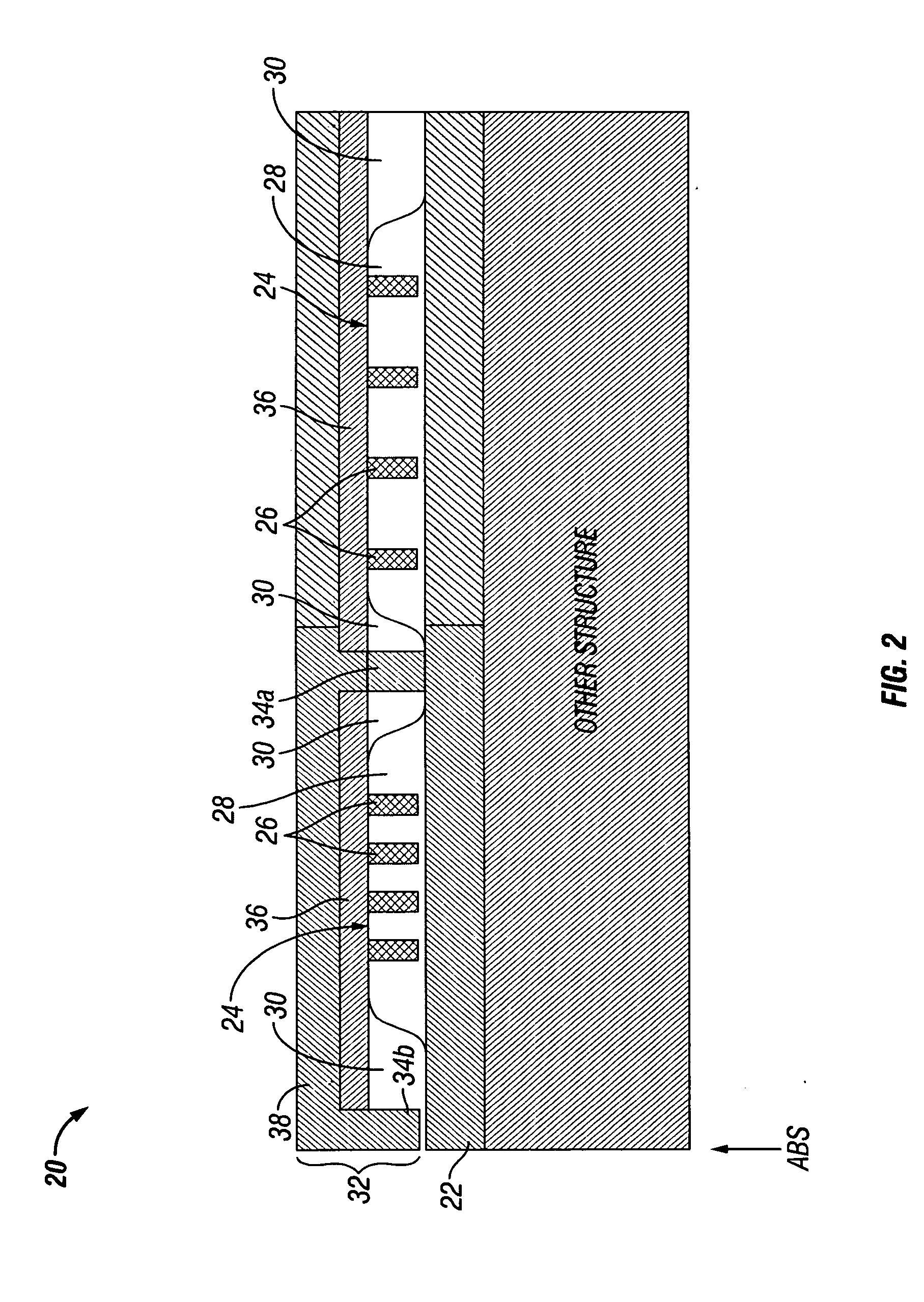
[0030] The slurry of this example was based on a commercially available product sold under the name “SC-112” by Cabot Microelectronics, Corporation. As sold, this slurry product comprises water and about 12% (by volume) silica abrasive having a particle size of less than 1000 Angstroms. The abrasive content of the SC-112 slurry was diluted to 9% abrasive content (by volume) by adding an ammonium persulfate / water mixture containing 10 grams / liter ammonium persulfate to produce the desired concentration of about 1.5-3 grams / liter ammonium persulfate in the slurry as a whole. A wafer comprising the structure shown in FIG. 3 was placed on a Strasbaugh model 6DS-SP CMP tool equipped with a standard polishing pad. Note that the hardbaked resist material 28 was hardbaked resist 1529. The polishing conditions were 6 psi down force, 50 rpm spindle speed, 35 rpm table speed and 110 ml / minute slurry flow. Under these conditions, it was observed that the NiFe P2 stubs 34a / 34b and the copper coi...

example 2

[0031] The slurry of this example was the same as that used in Example 1 except that 0.5% (by volume) of TRITON® X100 surfactant was added. A wafer containing the structure shown in FIG. 3 was placed on a Strasbaugh model 6EC CMP tool (similar to the Strasbaugh model 6DS-SP CMP tool of Example 1) equipped with a standard polishing pad. As in Example 1, the hardbaked resist material 28 was hardbaked resist 1529. The polishing conditions were 6 psi down force, 40 rpm spindle speed, 41 rpm table speed and 110 ml / minute slurry flow. Both the NiFe P2 stubs 34a / 34b and the copper coils 26 were exposed after seven minutes forty seconds of polishing time. The planarization results are shown by Table 2 below, which sets forth the differences in height of the various materials of the planarized head 20 of FIG. 4.

TABLE 2STEP LOCATIONSTEP SIZENiFe back gap P2 stub / hardbaked resist1600ANiFe back gap P2 stub / alumina700AWide pitch copper coils / hardbaked resist150ANarrow pitch copper coils / hardba...


PUM

PropertyMeasurementUnit
concentrationaaaaaaaaaa
particle sizeaaaaaaaaaa

Abstract

A method for simultaneously planarizing to relatively equal smoothness a thin film magnetic head hardbaked resist structure having relatively low surface energy and one or more additional thin film magnetic head structures containing other materials having comparatively higher surface energy, such as copper, hardbaked resist, alumina and NiFe. The method begins with preparation of a chemical mechanical polishing (CMP) slurry targeted at equaling the removal rate of the materials to be planarized. The CMP slurry includes a liquid vehicle, an abrasive, and a surfactant. The CMP slurry is applied to the surface of the structures to be planarized and the structures are simultaneously planarized using a CMP planarization technique.

Description

BACKGROUND OF THE INVENTION [0001] 1. Field of the Invention [0002] The present invention relates to thin film heads for magnetically writing information on data storage media, and particularly to fabrication processes for manufacturing such heads. Still more particularly, the invention concerns the planarization of device layer surfaces in thin film magnetic write heads using chemical mechanical polishing techniques. [0003] 2. Description of the Prior Art [0004] By way of background, thin film magnetic write heads conventionally include a P2 pole piece having a sloping surface that extends toward the pole tip area where the head's write gap is located. An example of this conventional geometry is shown in the FIG. 1, which illustrates a side view of a prior art write head 2 in which the ABS (Air Bearing Surface) of the head is on the right side of the figure. The P2 pole piece 4 lies over an integrated layer 6 containing plural copper coils 8 surrounded by insulative hard bake resis...

Claims


Application Information

Patent Timeline
Patent Type & Authority Applications(United States)
IPC IPC(8): B24B7/30B24B37/04C09G1/02G11B5/127
CPCB24B37/044C09G1/02Y10T29/49048Y10T29/49041Y10T29/49032G11B5/1276
Inventor ESCHBACH, FLORENCELEE, ERIC JAMESPOWELL PHIPPS, PETER BEVERLEYBAER, AMANDAPONG LEE, EDWARD HINMARTIN, FRANCISCO
Owner HITACHI GLOBAL STORAGE TECH NETHERLANDS BV
Learn More