Non-volatile memory device

a memory device and non-volatile technology, applied in the direction of data conversion, digital storage, generating/distributing signals, etc., can solve the problem of circuit size increasing, and achieve the effect of reducing the size of the region

Active Publication Date: 2006-05-11
INFINEON TECH LLC
View PDF14 Cites 31 Cited by
  • Summary
  • Abstract
  • Description
  • Claims
  • Application Information

AI Technical Summary

Benefits of technology

[0017] According to the present invention, the non-volatile memory device for reading out the previously-stored operational information and transferring it to the volatile memory section for retention is provided with the first volatile memory section configured with compact-sized circuits selected depending on the identification information and the second volatile memory section configured with a sufficient electric current-driving capacity so as to constantly conduct logical processing, thus making it possible to store the operational information in a desirable volatile memory section depending on the attributes of the operational information. It is also possible to drastically reduce the size of the region of the volatile memory section which stores all the operational information.

Problems solved by technology

Thus, it is disadvantageous to retain operational information such as write-protect information required only under specific conditions in a volatile memory region similar in configuration to the initialization data latch circuits 230 and 250, and the chip information data latch circuit 280, considering the circuit size requirements of the data latch circuits 230, 250, 280, which are provided and configured with latch circuit LA, et al.
The circuit thus becomes larger in size to enable the electric current-driving capacity, posing problems.

Method used


Image

  • Non-volatile memory device
  • Non-volatile memory device
  • Non-volatile memory device

Examples


Embodiment Construction

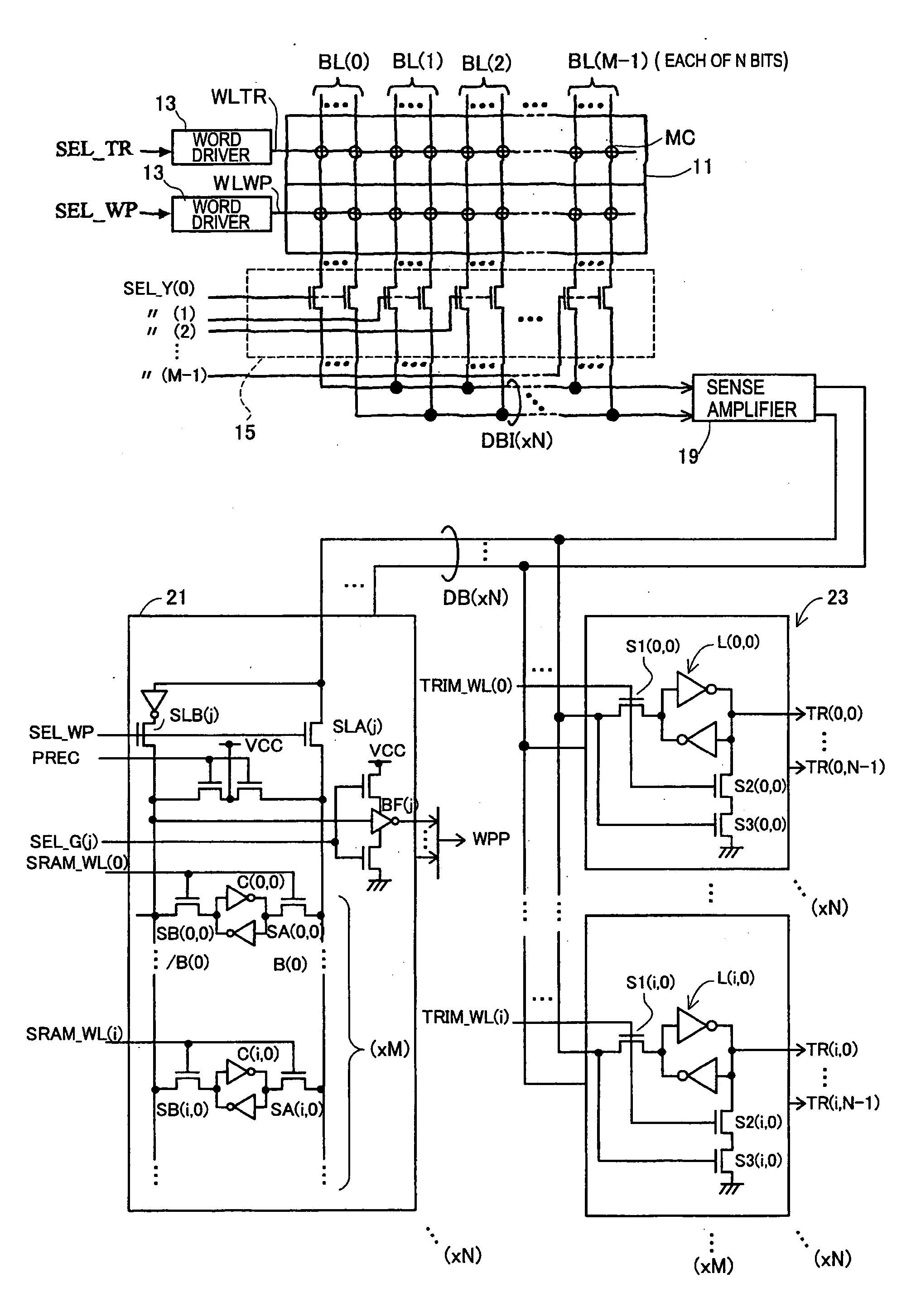
[0029] Hereinafter, a detailed explanation will be made for the specific embodiments of the non-volatile memory device in the present invention by referring to FIGS. 1 to 8.

[0030] In a non-volatile memory device, operating conditions in operating circuits are set according to various types of operational information. The operational information is mainly classified into two types.

[0031] The first type of operational information is information set by vendors before shipment of the products. This information is necessary for allowing a non-volatile memory device to execute certain operations and includes information for adjusting bias voltage values which are used in various operations such as program operations, erase operations and read-out operations, information for adjusting the operation timing of various operations, information for adjusting the oscillation frequency of built-in oscillators, and redundant address information for redundantly saving defective memory cells. Thes...


PUM


Abstract

The operational information read out by the read-out sense amplifier (19) is transferred via the data line DB to a volatile memory section. The volatile memory section is configured with the volatile memory section (21) having a SRAM configuration and the second volatile memory section (23) configured with latch circuits, which are respectively connected in parallel with the data line DB. The operational information, which may be provided depending on an operation state of the write-protect information and other information stored in the non-volatile memory cell MC selected by the word line WLWP, is written and read out with respect to the first volatile memory section (21) in response to the identification information linked with the operational information. The operational information which must be constantly accessible, is written into the second volatile memory section (23) in response to the identification information. Thus, the operational information is available in a memory mode depending on the attributes of the operational information.

Description

CROSS-REFERENCES TO RELATED APPLICATIONS [0001] This is a continuation of International Application No. PCT / JP2004 / 015833, filed Oct. 26, 2004 which was not published in English under PCT Article 21(2).TECHNICAL FIELD [0002] The present invention relates to a non-volatile memory device in which operational information is stored and, in particular, relates to a non-volatile memory device wherein the previously-stored operational information is read out according to an initialization operation and retained in a referable state. BACKGROUND ART [0003] In the non-volatile semi-conductor memory device disclosed in Japanese Unexamined Patent Publication No. 2001-176290 (Patent Document 1), as shown in FIG. 9, an initialization data region 130 of a memory cell array 110 is provided for a cell block, a minimum unit of data erase, and predefined as a region to write initialization data for deciding the operating conditions of the memory. [0004] A power-on reset circuit 270 is operated in resp...

Claims


Application Information

Patent Timeline
IPC IPC(8): G06F1/04
CPCG11C7/20G11C7/24G11C8/08G11C11/417G11C16/20G11C16/225G11C29/028G11C2029/4402
Inventor NAGAO, MITSUHIROKATO, KENTA
Owner INFINEON TECH LLC
Why Eureka
Try Eureka