

Semiconductor device
a technology of semiconductor devices and semiconductors, applied in the direction of semiconductor devices, electrical equipment, transistors, etc., can solve the problems of requiring a long time for epitaxial growth and the inability to meet the requirements of epitaxial growth
- Summary
- Abstract
- Description
- Claims
- Application Information
AI Technical Summary
Benefits of technology
Problems solved by technology
Method used
Image

Examples
first embodiment
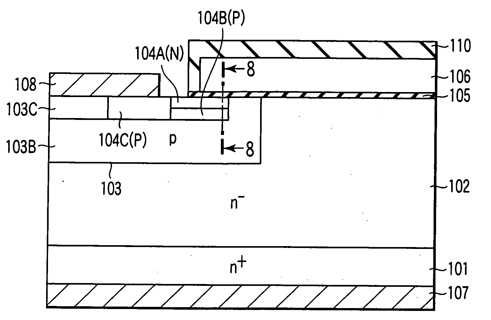
[0060]FIG. 1 is a sectional view showing a configuration of a DIMOSFET according to a first embodiment of the present invention. In FIG. 1, an SiC layer (n− layer) 102 including an n-type impurity concentration of 5×10¹⁵ to 2×10¹⁶ / cm3 and having a thickness of about 5 to 10 μm is formed on a hexagonal SiC substrate (n+ substrate) 101 including n-type impurities at an impurity concentration of about 5×10¹⁸ to 1×10¹⁹ / cm3. On a partial surface of the SiC layer 102, there is formed a first silicon carbide region 103 (p-type well) whose p-type impurity concentration is about 1×10¹⁷ to 5×10¹⁷ / cm3 and which exists in a region from the SiC layer 102 surface to a depth of 0.6 μm. This p-type well constitutes the p-type base area 103. It is to be noted that a combination of base sub-areas 103B and 103C is generically referred to as the p-type base area 103.
[0061] Moreover, an n-type source region 104 (104A, 104B, 104C) is formed as a second silicon carbide region in this p-type base area 103...
second embodiment
[0094]FIG. 21 is a sectional view showing a configuration of a UMOSFET according to a second embodiment of the present invention. In FIG. 21, an SiC layer 202 including an n-type impurity concentration of about 5×10¹⁵ / cm3 and having a thickness of about 10 μm is formed on a hexagonal SiC substrate 201 including n-type impurities in an impurity concentration of about 5×10¹⁹ / cm3. On the partial surface of the SiC layer 202, there is formed a channel region (first silicon carbide region) 203 (generic term of 203B, 203C) whose p-type impurity concentration is about 1×10¹⁷ to 5×10¹⁷ / cm3 and which has a thickness of about 2 μm.
[0095] Moreover, an n-type source region 204 is formed on this channel region 203B. In more detail, a first source sub-region 204A containing nitrogen as n-type impurity in a range of 1×10¹⁸ to 1×10²⁰ / cm3 is selectively formed. Outside the first source sub-region 204A, there is formed a second source sub-region 204B containing about 1×10²⁰ / cm3 of phosphorus (P) as ...
third embodiment
[0116]FIG. 34 is a sectional view showing a configuration of a lateral MOSFET according to a third embodiment of the present invention. The embodiment may be basically considered as a lateral type of DIMOSFET of the first embodiment. A p-type base region (first silicon carbide region) 303 and a second silicon carbide region 304 provided in the base region are selectively (on the left side of FIG. 34) formed on an n-type silicon carbide substrate 309(N) to which nitrogen has been added in the same manner as in the first embodiment. A low-concentration third silicon carbide region 302(N) to which nitrogen has been added is formed adjacent to and in contact with this p-type base region 303 on the silicon carbide substrate 309.
[0117] As described above, the n-type source region 304 is formed on the surface of the p-type base region 303 in the same manner as in the first embodiment. The n-type source region 304 includes a first source sub-region 304A(N), a second source sub-region 304C(...
PUM
 Abstract
Description
Claims
Application Information