

Solid-state image device and camera including solid-state image device
a solid-state image and image technology, applied in the field of solid-state image devices, can solve the problems of more severe problems than maintaining known battery longevity, new technological problems, and dark current non-uniformity on the screen, and achieve excellent quality and reduce dark current non-uniformity
- Summary
- Abstract
- Description
- Claims
- Application Information
AI Technical Summary
Benefits of technology
Problems solved by technology
Method used
Image

Examples
first embodiment
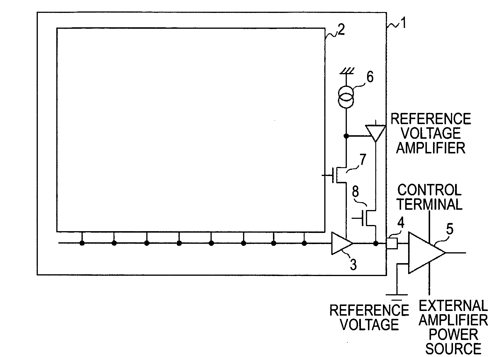
[0040]FIG. 1 is a schematic diagram schematically showing a solid-state image device according to a first embodiment of the present invention.
[0041] Reference numeral 1 denotes the entire solid-state image device. Pixels each including a photoelectric converter are arranged two-dimensionally in a pixel area 2. An output amplifier 3 outputs signals of the pixels. An external amplifier (provided with a control terminal) 5 is disposed near an output terminal 4. Reference numeral 6 denotes a current source of the output amplifier 3. A power-save switch 7 reduces the current consumption of the output amplifier 3. Reference numeral 8 denotes an output selection switch. These units are arranged as shown in FIG. 1.
[0042] A structure in which the external amplifier 5 is added to the solid-state image device 1 can also be referred to as a solid-state image device in terms of functionality. This is also applied to the embodiments described below.
[0043] In the first embodiment, during an acc...
second embodiment
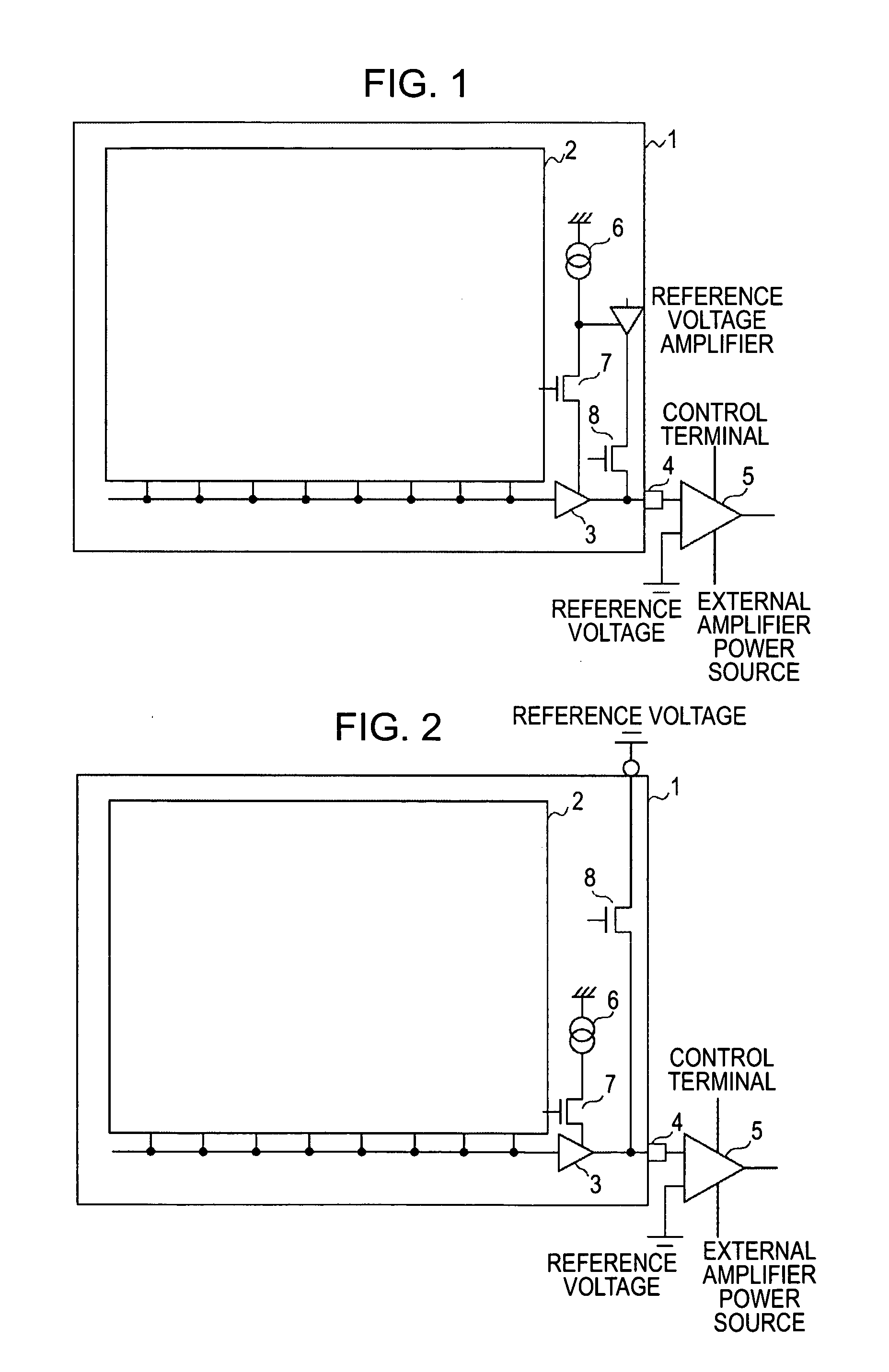
[0048]FIG. 2 is a schematic diagram schematically showing a solid-state image device according to a second embodiment of the present invention.
[0049] Reference numeral 1 denotes the entire solid-state image device. Pixels each including a photoelectric converter are arranged two-dimensionally in a pixel area 2. An output amplifier 3 outputs signals of the pixels. An external amplifier (provided with a control terminal) 5 is disposed near an output terminal 4. Reference numeral 6 denotes a current source of the output amplifier 3. A power-save switch 7 reduces the current consumption of the output amplifier 3. Reference numeral 8 denotes an output selection switch.
[0050] In the second embodiment, during an accumulation time, the current consumption of the output amplifier 3 is reduced using the power-save switch 7, and an increase in the dark current of a photoelectric converter located near the output amplifier 3 is thus suppressed. In addition, in order to reduce the current cons...
third embodiment
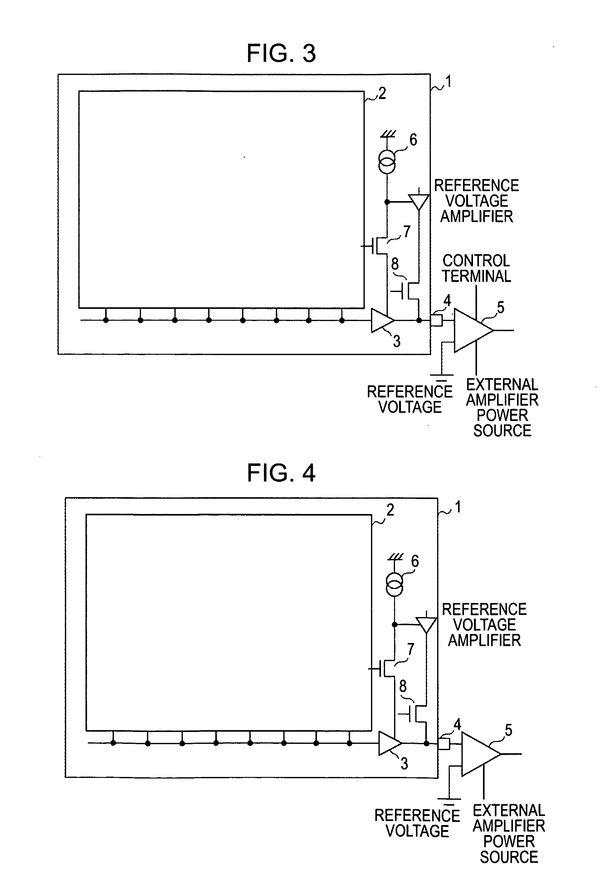
[0055]FIG. 3 is a schematic diagram schematically showing a solid-state image device according to a third embodiment of the present invention.
[0056] Reference numeral 1 denotes the entire solid-state image device. Pixels each including a photoelectric converter are arranged two-dimensionally in a pixel area 2. An output amplifier 3 outputs signals of the pixels. An external amplifier (provided with a control terminal) 5 is disposed near an output terminal 4. Reference numeral 6 denotes a current source of the output amplifier 3. A power-save switch 7 reduces the current consumption of the output amplifier 3. Reference numeral 8 denotes an output selection switch. These units are arranged as shown in FIG. 3.
[0057] In the third embodiment, during an accumulation time, the current consumption of the output amplifier 3 is reduced using the power-save switch 7, and an increase in the dark current of a photoelectric converter located near the output amplifier 3 is thus suppressed. In ad...
PUM
 Abstract
Description
Claims
Application Information