

Remote plasma activated nitridation
a plasma activation and remote technology, applied in the direction of coatings, chemical vapor deposition coatings, semiconductor devices, etc., can solve the problems of difficult control of conventional methods of incorporating nitrogen into gate dielectrics, and the amount of incorporated nitrogen may be less than desired in some applications
- Summary
- Abstract
- Description
- Claims
- Application Information
AI Technical Summary
Problems solved by technology
Method used
Image

Examples
example 1
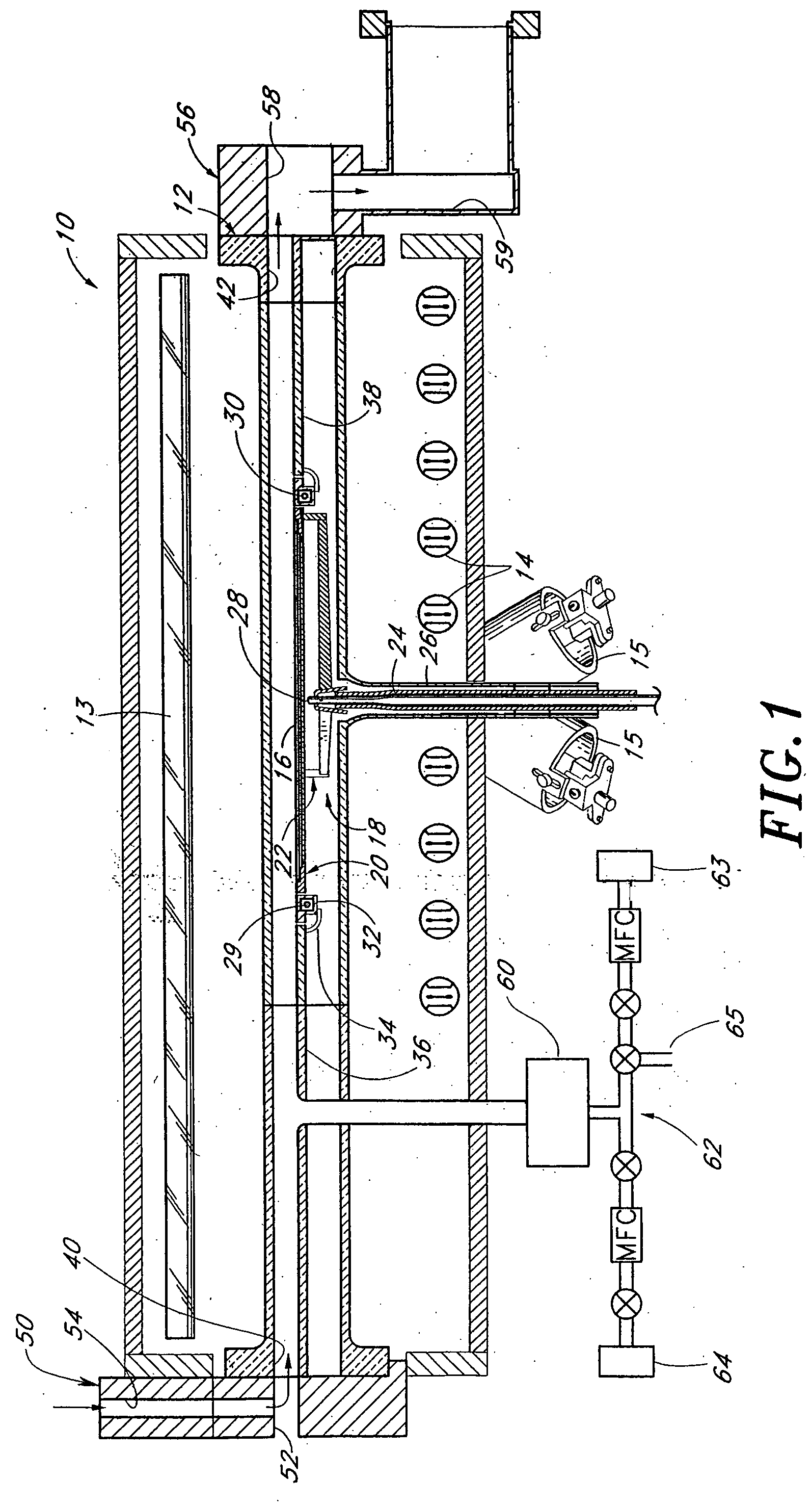
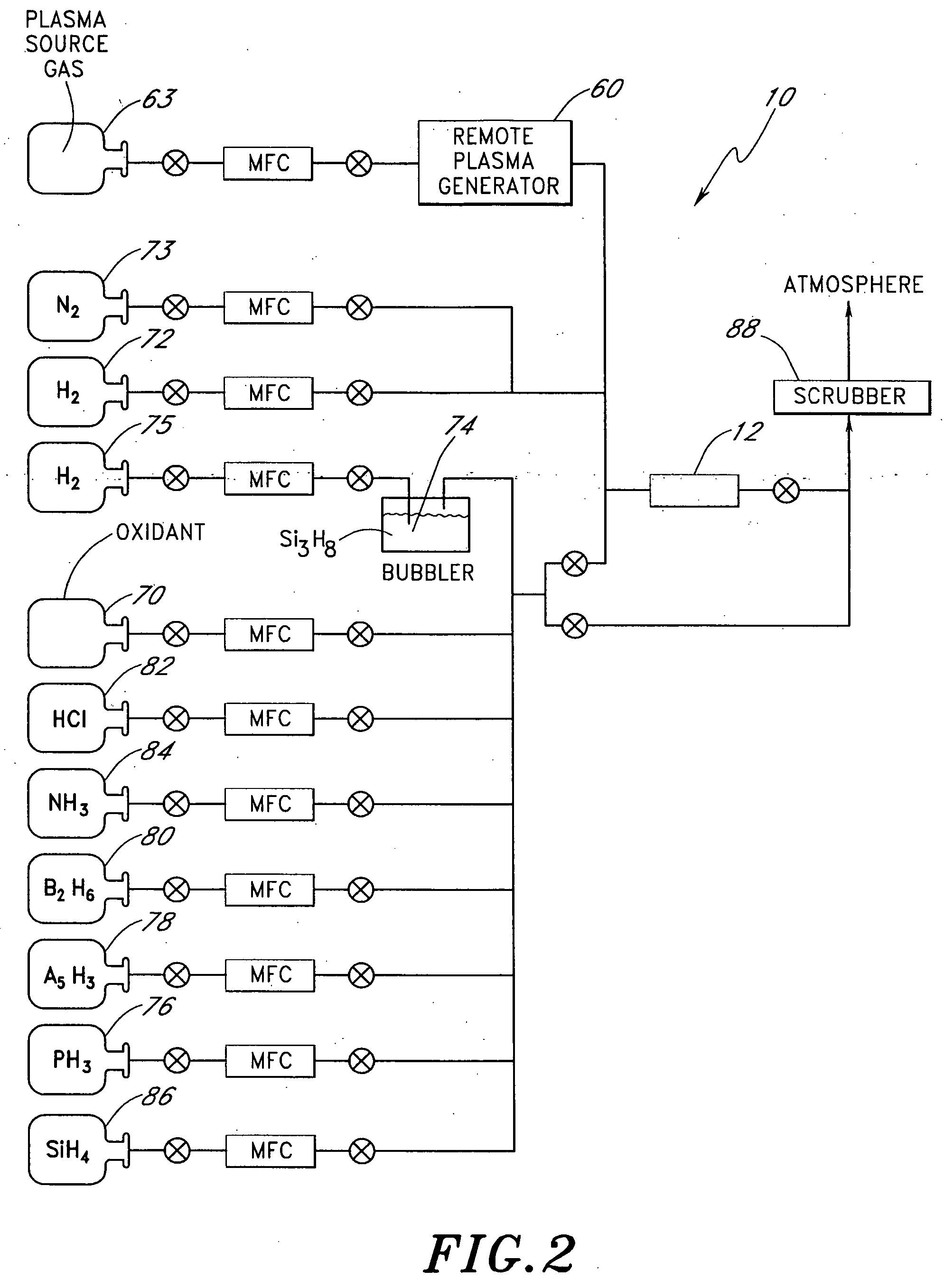
[0061] The effect of adding NH3 downstream of a N2 plasma source in a remote plasma enhanced chemical vapor deposition (RPECVD) of a silicon nitride film was investigated. The deposition was performed in a single substrate Epsilon™ reactor from ASM America, Inc. of Phoenix, Ariz. A wafer was loaded into the reaction chamber and prepared for silicon nitride deposition. The deposition temperature was set at 650° C. and the pressure at 2 Torr. Silane (SiH4) was used as the silicon precursor and was flowed into the reaction chamber at 10 sccm. Ammonia was flowed into the reaction chamber at rates that varied from 0-1000 sccm, depending upon the deposition run. Excited nitrogen species, comprising nitrogen radicals and metastable nitrogen species, were generated by flowing nitrogen gas (N2) into a microwave radical generator (MRG) at 4 slm and flowed into the reaction chamber. In depositions where ammonia was flowed into the chamber, the flow of the excited nitrogen species was merged wi...
example 2
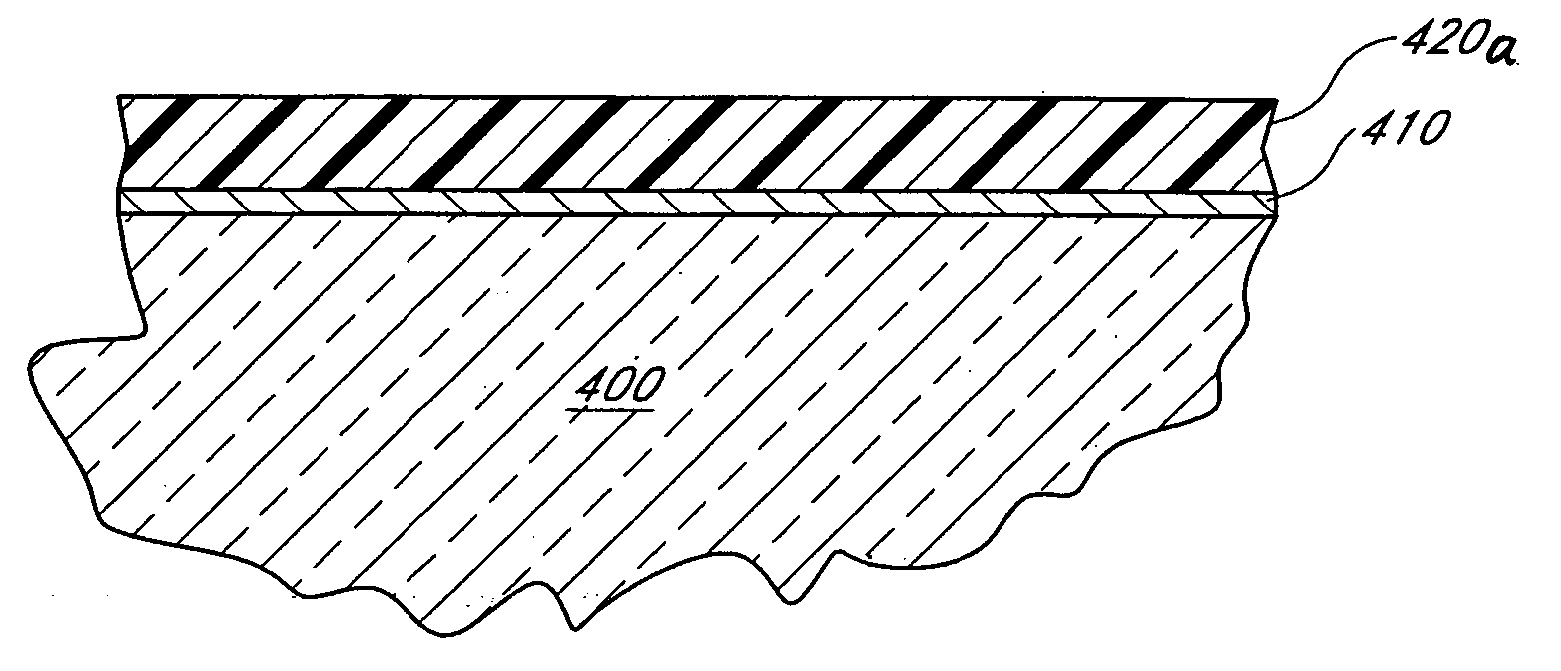
[0064] The effect of adding NH3 downstream of a N2 plasma source to incorporate nitrogen into an already-formed high-k dielectric was investigated. The nitrogen incorporation was performed in a single substrate Epsilon™ reactor from ASM America, Inc. of Phoenix, Ariz. Nitrogen was incorporated into a 2 nm HfSiO layer (Hf:Si pulse ratio of 1:1) in various post deposition anneals.
[0065] Depositions by thermal nitridation at a temperature of 700° C. using NH3 were used as a reference. The partial pressure of the NH3 was varied from about 0.05 to about 1.2 Torr.
[0066] In other experiments, remotely excited nitrogen species derived from N2 were flowed into the reaction chamber along with a flow of NH3. The nitridation temperature was set at 600° C. The pressure was held constant at 2.5 Torr. Excited nitrogen species were generated by flowing nitrogen gas into a microwave radical generator (MRG) at 16 slm. Ammonia was flowed into the reaction chamber at rates varying from 0.2 slm to 2 s...
PUM
| Property | Measurement | Unit |
|---|---|---|
| temperature | aaaaa | aaaaa |
| temperature | aaaaa | aaaaa |
| total volume capacity | aaaaa | aaaaa |
Abstract
Description
Claims
Application Information