High-voltage transistor device having an interlayer dielectric etch stop layer for preventing leakage and improving breakdown voltage

a dielectric and high-voltage transistor technology, applied in the direction of transistors, semiconductor devices, electrical equipment, etc., can solve the problems of gate oxide breakdown voltage, silicon-rich sion film is not sufficient for buffer isolation in high-voltage device applications, and the process of high-voltage device compatible with current low-voltage device processes and middle-voltage device processes is an important issue, so as to prevent leakage and improve breakdown voltage

Active Publication Date: 2006-06-01
TAIWAN SEMICON MFG CO LTD
View PDF8 Cites 83 Cited by
  • Summary
  • Abstract
  • Description
  • Claims
  • Application Information

AI Technical Summary

Benefits of technology

[0005] Embodiments of the present invention include high-voltage transistor devices having an interlayer dielectric (ILD

Problems solved by technology

Since devices with different breakdown voltages are required on a single chip, making the high-voltage device process compatible with current low-voltage device processes and middle-voltage device processes has become an important issue.
Such a silicon-rich SiON film is insufficient for buffer isolation in high-voltage device applications because the silicon-rich SiON film generates an extr

Method used


Image

  • High-voltage transistor device having an interlayer dielectric etch stop layer for preventing leakage and improving breakdown voltage
  • High-voltage transistor device having an interlayer dielectric etch stop layer for preventing leakage and improving breakdown voltage
  • High-voltage transistor device having an interlayer dielectric etch stop layer for preventing leakage and improving breakdown voltage

Examples


Embodiment Construction

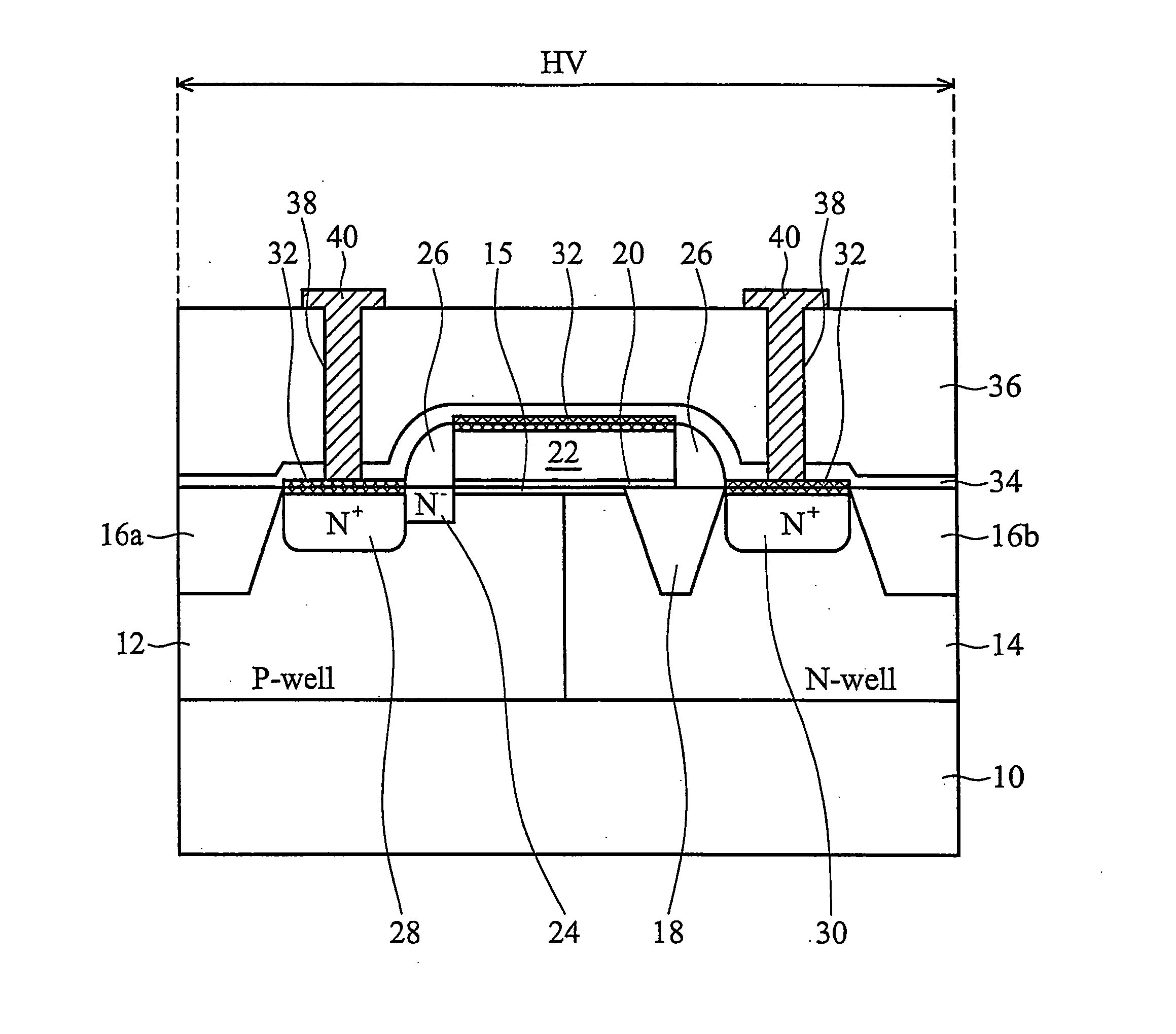
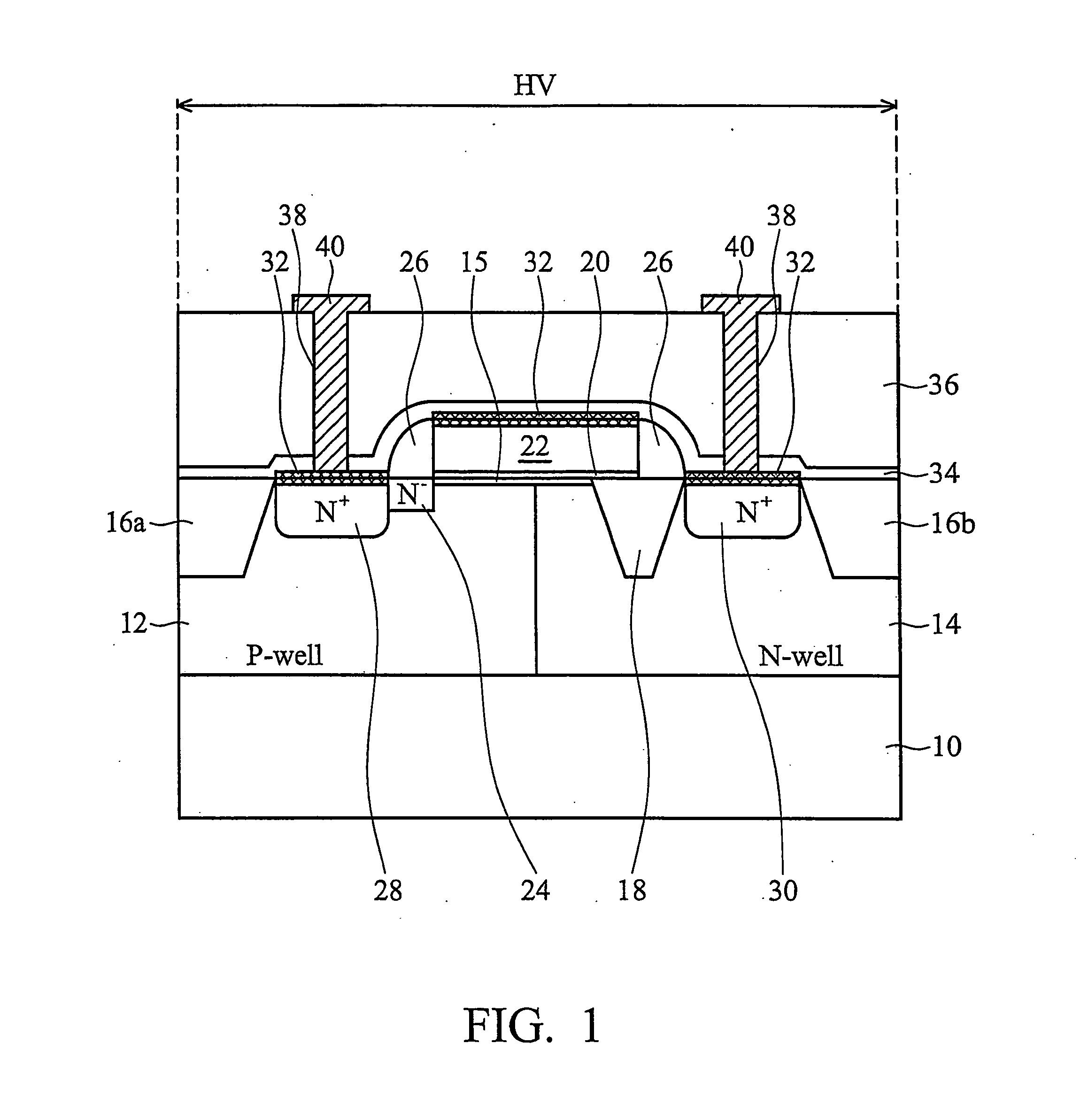
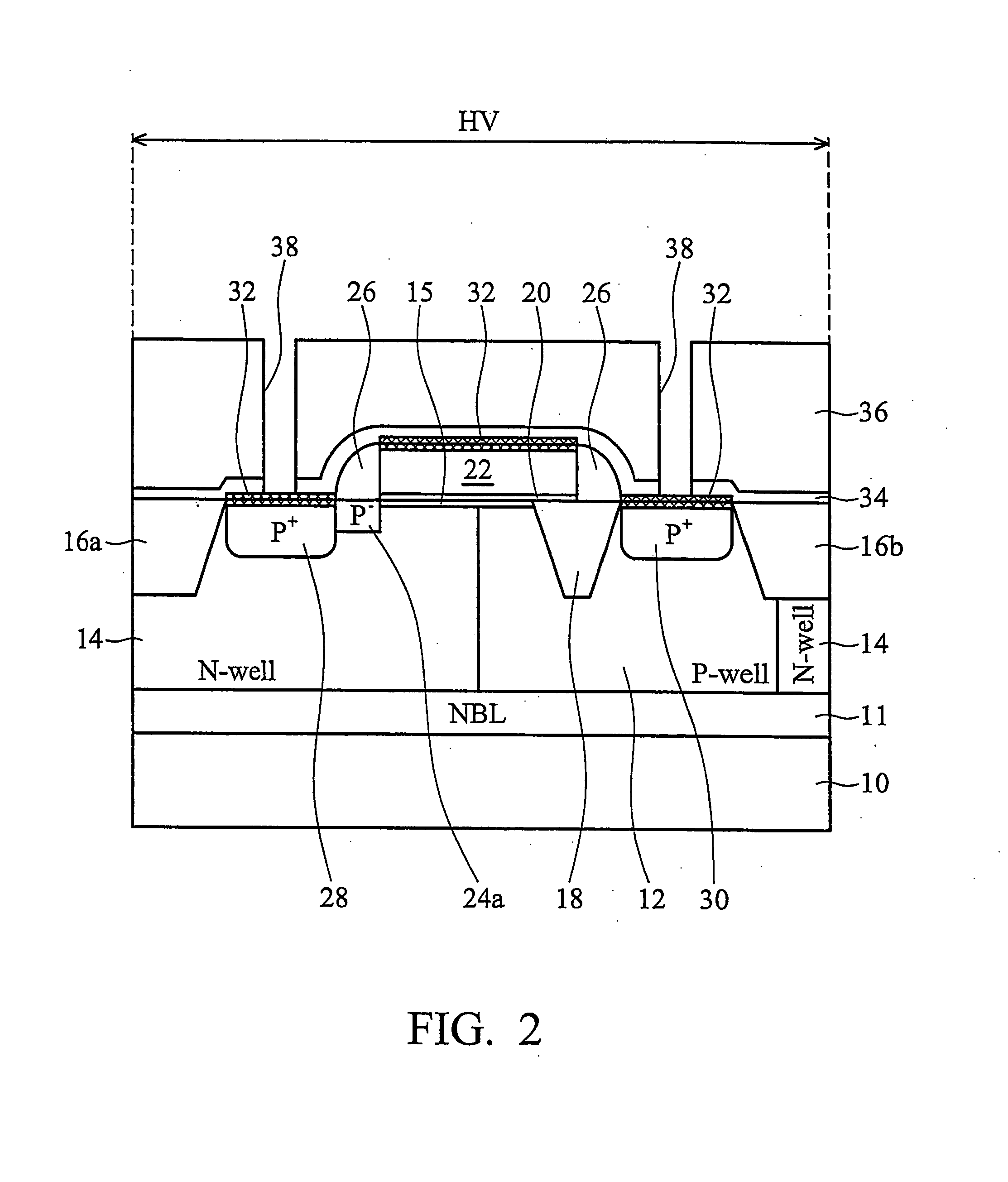
[0019] Preferred embodiments of the present invention provide high-voltage transistor devices with an interlayer dielectric (ILD) etch stop layer for use in a subsequent contact hole process. The etch stop layer of the preferred embodiments is selected from any dielectric material other than silicon-rich SiON, which overcomes the aforementioned problems of the prior art arising from the use of a silicon-rich SiON etch stop layer. Particularly, the invention provides a high-resistivity dielectric film having a resistivity greater than 10 ohm-cm as an etch stop layer beneath an ILD layer for fabricating a contact hole in a high-voltage device process, which achieves desired buffer isolation to prevent leakage when driving a high voltage e.g., greater than 5V, at the gate site of the high-voltage transistor device. The high-resistivity dielectric film can suppress an extra leakage path from gate site to source site, and the gate oxide breakdown voltage can therefore be improved to pass...


PUM


Abstract

A high-voltage transistor device with an interlayer dielectric (ILD) etch stop layer for use in a subsequent contact hole process is provided. The etch stop layer is a high-resistivity film having a resistivity greater than 10 ohm-cm, thus leakage is prevented and breakdown voltage is improved when driving a high voltage greater than 5V at the gate site. A method for fabricating the high-voltage device is compatible with current low-voltage device processes and middle-voltage device processes.

Description

TECHNICAL FIELD [0001] The present invention relates to transistor devices for high-voltage applications, and particularly to a high-voltage transistor device with an interlayer dielectric (ILD) etch stop layer for preventing leakage and improving breakdown voltage. BACKGROUND [0002] High-voltage devices are highly desirable for numerous applications, including LCD (liquid crystal display) driver ICs, power management devices, power supplies, nonvolatile memories, communication circuits, and control circuits. Particularly, the LCD driver IC requires low-voltage / middle-voltage operation for driving an associated logic circuit together with high-voltage operation for driving the LCD during operation. Since devices with different breakdown voltages are required on a single chip, making the high-voltage device process compatible with current low-voltage device processes and middle-voltage device processes has become an important issue. [0003] In general, most high-voltage metal-oxide-se...

Claims


Application Information

Patent Timeline
IPC IPC(8): H01L29/00
CPCH01L21/76829H01L21/76832H01L29/0653H01L29/665H01L29/66659H01L29/66689H01L29/7816H01L29/7833H01L29/7835H01L29/7836
Inventor CHEN, CHUNG-IKUAN, HSINCHEN, ZHI-CHENGYEH, RANN-SHYANCHANG, CHI-HSUENLIU, JUNSUNG, TZU-CHIANGLIU, CHIA-WEICHANG, JIEH-TING
Owner TAIWAN SEMICON MFG CO LTD
Why Eureka
Try Eureka