

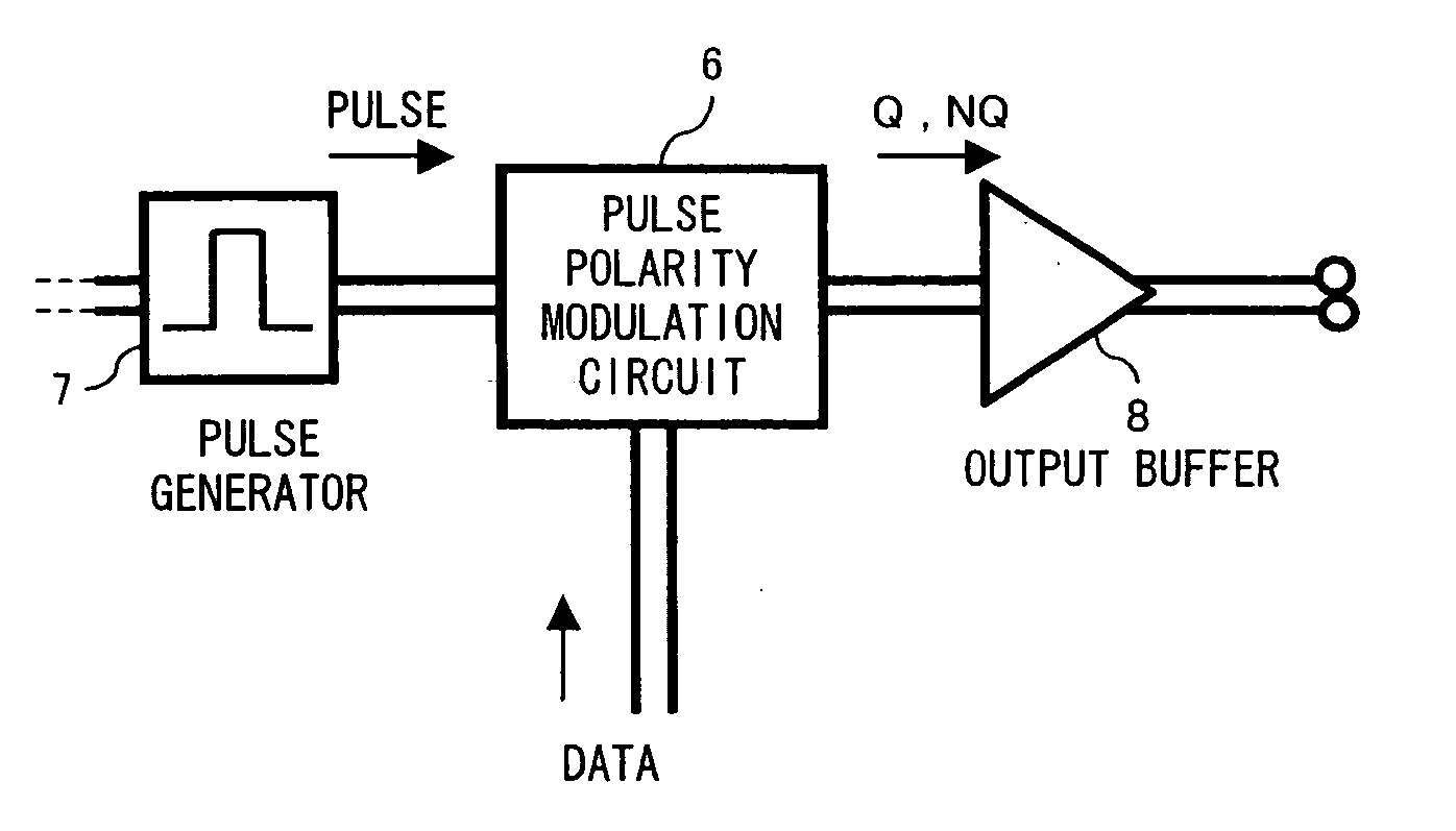
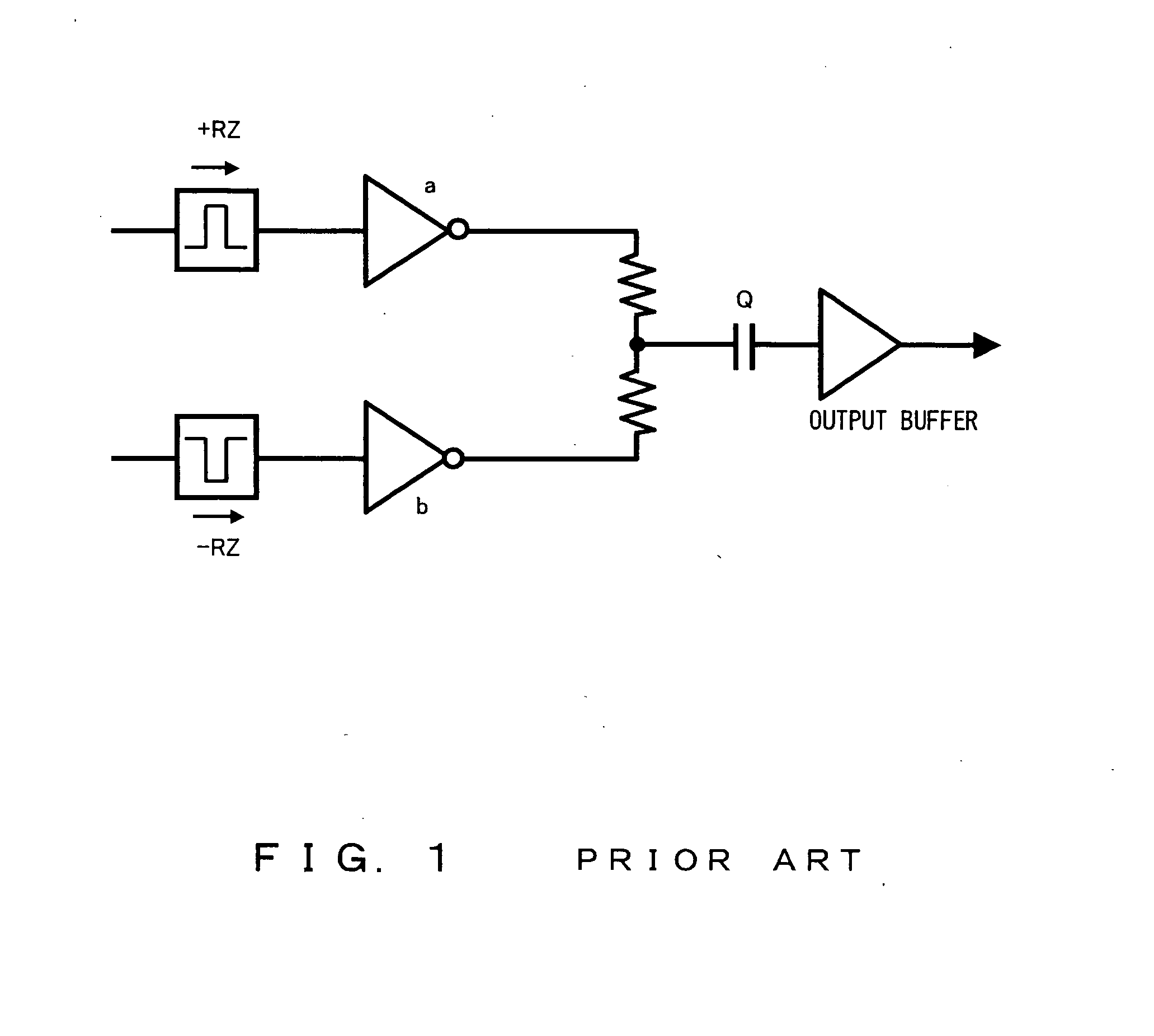
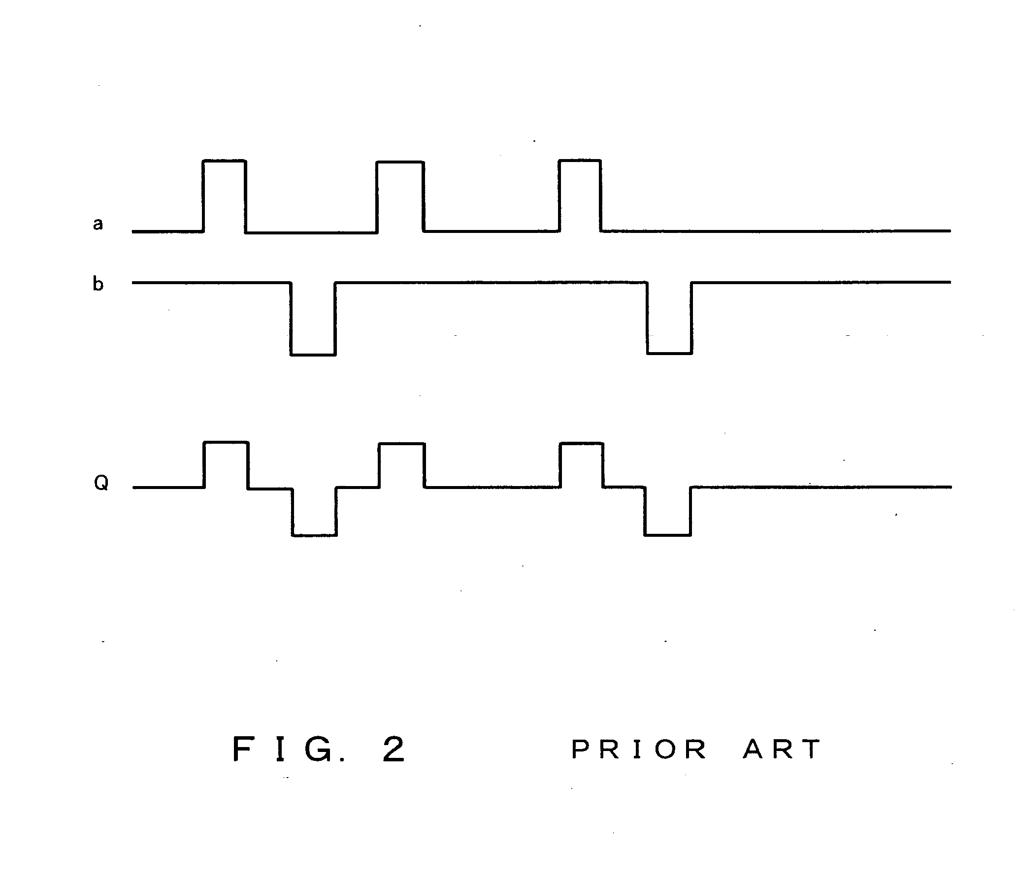
Pulse polarity modulation circuit
a technology of polarity modulation and pulse, applied in pulse manipulation, pulse frequency/rate modulation, pulse technique, etc., can solve the problems of large noise, difficulty in realizing low power consumption and space saving, etc., and achieve the effect of reducing noise and low power consumption
- Summary
- Abstract
- Description
- Claims
- Application Information
AI Technical Summary
Benefits of technology
Problems solved by technology
Method used
Image

Examples
Embodiment Construction
[0025]FIG. 3 is the principle block diagram of a pulse polarity modulation circuit according to the present invention. FIG. 3 shows the principle structure of the pulse polarity modulation circuit in which differential transistor pairs are double stacked and two transistors constituting a differential transistor pair 1 in a lower stage are coupled to their respective differential transistor pairs 2 and 3 in an upper stage.
[0026] In the pulse polarity modulation circuit according to the present invention, one of the differential transistor pairs in the upper stage, that is, the differential transistor pair 2 outputs polarity modulation pulses. The gates of the other differential transistor pair, that is, the differential transistor pair 3, are coupled together, and a middle potential between logic high and low is applied to the gates
[0027] Thus, in the pulse polarity modulation circuit according to the present invention, by applying the logic middle potential to the gates of the di...
PUM
 Abstract
Description
Claims
Application Information