Solder interconnect structure and method using injection molded solder

a technology of injection molded solder and interconnects, which is applied in the direction of soldering apparatus, sustainable manufacturing/processing, and final product manufacturing, etc., can solve the problems of thermal fatigue failure of the solder joints, and reduced spherical solder joints. , to achieve the effect of improving current carrying capacity, facilitating underfill reinforcement of the interconnects, and facilitating chip and substrate stando

Inactive Publication Date: 2006-06-08
IBM CORP
View PDF19 Cites 13 Cited by
  • Summary
  • Abstract
  • Description
  • Claims
  • Application Information

AI Technical Summary

Benefits of technology

[0009] It is another object of the invention to provide solder interconnects with greater standoff between chip and substrate to facilitate underfill reinforcement of the interconnects.
[0010] It is another object of the invention to provide solder interconn...

Problems solved by technology

These solder joints suffer thermal fatigue failures because of the difference in coefficient of thermal expansion (CTE) between the silicon and the chip carriers to which they are attached.
First, the spherical solder joints have limited fatigue life due to a difference in coefficient of thermal expansion between the silicon die and the substrate, often an organic material.
As the level of integration in silicon continues to increase, the number and density of solder interconnections also must increase, driving a reduction in size of the spherical solder joints and making it difficult or impossible for underfill to be used.
Second, silicon chip sizes are increasing, which also limits the ability of underfills to reinforce conventional spherical solder interconnects.
Third, power requirements for silicon devices are increasing, particularly for microprocessor chips; and conventional solder interconnects may not be able to withstand the ...

Method used


Image

  • Solder interconnect structure and method using injection molded solder
  • Solder interconnect structure and method using injection molded solder
  • Solder interconnect structure and method using injection molded solder

Examples


example 1

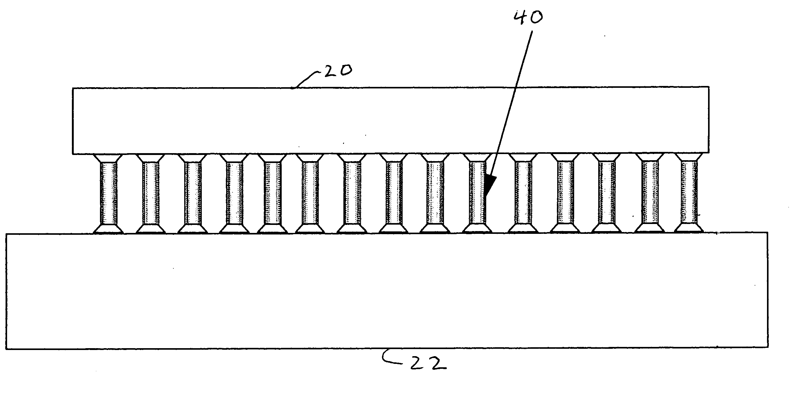
[0057] A preferred structure for improved flip chip interconnects may have cylindrical solder columns of diameter of 25-150 microns, preferably 50-100 microns. The interconnects may be 100-600 microns long, with an aspect ratio of length to diameter of 1.5:1-10:1, with a preferred range of 2:1 to 4:1. The method of fabrication of the interconnects can be described as follows.

[0058] A rectangular or square mold plate is patterned with an array of preferably cylindrical cavities. The mold plate can be of borosilicate glass, or be a composite of a laser machined polymer layer and glass, as disclosed in U.S. patent application Ser. No. 10 / ______, entitled Composite Solder Transfer Moldplate Structure and Method of Making Same, Attorney Docket No. YOR920030189US1, which is assigned to the same assigned as the present invention and is incorporated herein in its entirety. Further, the moldplate can be of a size to encompass a 200 mm or 300 mm wafer pattern such that the array of cavities ...

example 2

[0061] Another preferred structure for improved flip chip interconnects is one in which a copper wire of diameter 25-100 microns is embedded in a solder column of diameter 50-150 microns. The interconnects may be 100-600 microns long, with an aspect ratio of length to diameter of 1.5:1-10:1, with a preferred range of 2:1 to 4:1. The method of fabrication of the interconnects can be described as follows.

[0062] A rectangular or square mold plate is patterned with an array of preferably cylindrical cavities. The mold plate can be of borosilicate glass or be a composite of polymer and glass, as disclosed in U.S. patent application Ser. No. 10 / ______, entitled Composite Solder Transfer Moldplate Structure and Method of Making Same, Attorney Docket No. YOR920030189US1, which is incorporated herein in its entirety. Further, the moldplate is of a size to encompass a 200 mm or 300 mm wafer pattern such that the array of cavities exactly matches the array of electrical connection pads on the...


PUM


Abstract

Improved interconnects are produced by injection molded solder which fills mold arrays with molten solder so that columns that have much greater height to width aspect ratios greater than one are formed, rather than conventional flip chip bumps. The columns may have filler particles or reinforcing conductors therein. In the interconnect structures produced, the cost and time of a subsequent underfill step is reduced or avoided. The problem of incompatibility with optical interconnects between chips because underfills require high loading of silica fillers which scatter light, is solved, thus allowing flip chips to incorporate optical interconnects.

Description

FIELD OF THE INVENTION [0001] This invention relates to the field of solder interconnects formed between circuit devices and substrates forming the next layer of electrical interconnect. More specifically, the invention relates to improvements in injection molded solder technologies used to form solder bump interconnections, generally on silicon wafers. BACKGROUND OF THE INVENTION [0002] Semiconductor chips are commonly connected to other circuitry using solder bumps having a diameter of about 100 microns. These solder joints suffer thermal fatigue failures because of the difference in coefficient of thermal expansion (CTE) between the silicon and the chip carriers to which they are attached. Using the injection molded solder (IMS) technique, solder interconnects can be fabricated on semiconductor chips or chip carriers with controlled shape and composition to increase the fatigue life of the joints. Thus, this invention pertains to improvements of solder interconnections for better...

Claims


Application Information

Patent Timeline
IPC IPC(8): B23K35/12
CPCB23K35/26H01L24/11H01L24/12H01L2224/1308H01L2224/13082H01L2224/131H01L2224/13147H01L2224/13155H01L2224/13176H01L2224/13181H01L2224/13184H01L2224/1357H01L2224/13639H01L2224/13644H01L2224/13655H01L2924/01004H01L2924/01027H01L2924/01029H01L2924/01033H01L2924/01047H01L2924/01073H01L2924/01074H01L2924/01078H01L2924/01079H01L2924/01082H01L2924/01322H01L2924/14H05K3/3426H05K3/3436H05K3/3468H05K2201/10287H05K2201/10992H05K2203/0113H05K2203/0415H05K2203/128H01L2924/00014H01L2924/014H01L2924/00013H01L2924/01005H01L2924/01006H01L2924/01044H01L2224/13099H01L2224/16225H01L2224/32225H01L2224/73204H01L2924/00H01L2924/10253H01L2224/0554H01L2224/05568H01L2224/05573H01L2924/15787Y02P70/50H01L2224/05599H01L2224/0555H01L2224/0556
Inventor BUCHWALTER, STEPHEN L.FEGER, CLAUDIUSGRUBER, PETER A.KANG, SUNG K.LAURO, PAUL A.SHIH, DA-YUAN
Owner IBM CORP
Why Eureka
Try Eureka