Semiconductor light emitting device having textured structure and method of manufacturing the same

a technology of light-emitting devices and semiconductors, which is applied in the direction of semiconductor devices, basic electric elements, electrical equipment, etc., can solve the problems of difficult growth of semiconductor layers with uniform quality, and reducing light extraction efficiency, so as to improve light extraction efficiency and reduce internal crystal defects

Active Publication Date: 2006-06-08
SAMSUNG ELECTRONICS CO LTD
View PDF10 Cites 55 Cited by
  • Summary
  • Abstract
  • Description
  • Claims
  • Application Information

AI Technical Summary

Benefits of technology

[0011] The present invention may provide a semiconductor light emitting diode having a structure that can improve light extraction efficiency and reduce internal crystal defects of the semiconductor light emitting diode and a method of manufacturing the semiconductor light emitting diode.

Problems solved by technology

If the light enters at an angle greater than the predetermined angle, the light totally is internally reflected at the flat interface, thereby greatly reducing the light extraction efficiency.
However, particularly as depicted in FIG. 1B, when the textured structure 120 is incorporated by patterning the sapphire substrate 111, the growth of a semiconductor layer with a uniform quality is difficult, because there is a great possibility of generating defects in the semiconductor layer due to unmatched crystal structure between the sapphire substrate 111 and the semiconductor layer formed on the sapphire substrate 111.
As a result, the light extraction efficiency is reduced due to the internal crystal defects.

Method used


Image

  • Semiconductor light emitting device having textured structure and method of manufacturing the same
  • Semiconductor light emitting device having textured structure and method of manufacturing the same
  • Semiconductor light emitting device having textured structure and method of manufacturing the same

Examples


Embodiment Construction

[0034] The present invention will now be described more fully with reference to the accompanying drawings in which exemplary embodiments of the invention are shown.

[0035]FIGS. 2 and 3 are cross-sectional views of semiconductor light emitting diodes having a textured structure according to the present invention.

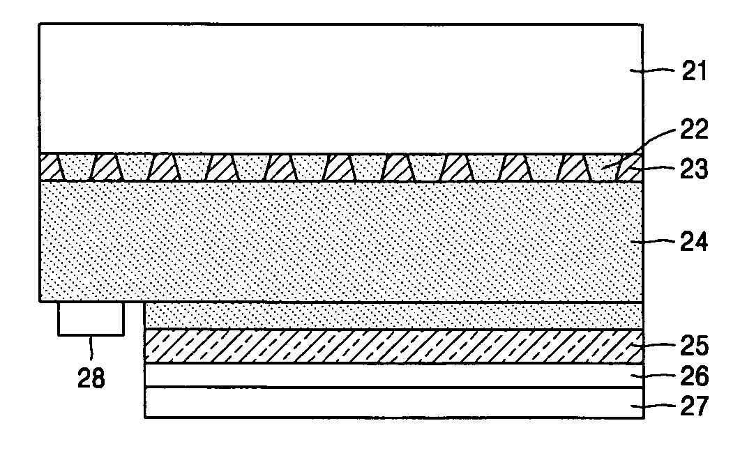
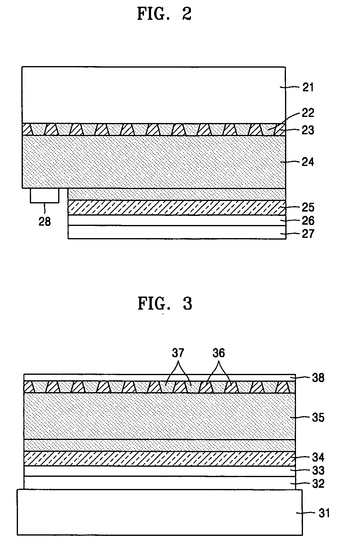
[0036]FIG. 2 shows a textured structure applied to flip-chip type semiconductor light emitting diodes and FIG. 3 shows a textured structure applied to vertical type semiconductor light emitting diodes.

[0037] Referring to FIG. 2, a first semiconductor layer 22 and an intermediate layer 23 are formed in a textured structure on a transparent substrate 21, and a second semiconductor layer 24 is formed on the first semiconductor layer 22 and the intermediate layer 23. An active layer 25, a third semiconductor layer 26 and a first electrode 27 are sequentially formed on a first region of the second semiconductor layer 24. A second electrode 28 is formed on a second region of the ...


PUM


Abstract

A semiconductor light emitting diode having a textured structure and a method of manufacturing the same are provided. The semiconductor light emitting diode includes a first semiconductor layer formed into a textured structure, an intermediate layer formed between the textured structures of the patterned first semiconductor layer, and a second semiconductor layer, an active layer, and a third semiconductor layer sequentially formed on the first semiconductor layer and the intermediate layer.

Description

CROSS-REFERENCE TO RELATED PATENT APPLICATION [0001] This application claims the benefit of Korean Patent Application No. 10-2004-0103112, filed on Dec. 8, 2004, in the Korean Intellectual Property Office, the disclosure of which is incorporated herein in its entirety by reference. BACKGROUND OF THE DISCLOSURE [0002] 1. Field of the Disclosure [0003] The present disclosure relates to a semiconductor light emitting diode, and more particularly, to a semiconductor light emitting diode that improves light extraction efficiency using a textured structure and a method of manufacturing the same. [0004] 2. Description of the Related Art [0005] A light emitting diode (LED) is a device used for converting electrical energy into infra red rays, visible light, or other light using the characteristics of a compound semiconductor. The light emitting diode is a type of electro luminescent (EL) device, and presently, the light emitting diodes that employ an III-V group compound semiconductor are b...

Claims


Application Information

Patent Timeline
Patent Type & Authority Applications(United States)
IPC IPC(8): H01L21/00H01L33/00H01L33/22H01L33/32H01L33/62
CPCH01L33/007H01L33/12H01L33/20H01L33/025H01L33/22
Inventor LEE, JEONG-WOOKSUNG, YOUN-JOONPAEK, HO-SUN
Owner SAMSUNG ELECTRONICS CO LTD
Why Eureka
Try Eureka