Reduced capacitance resistors

a capacitance resistor and parasitic capacitance technology, applied in the field of resistors, can solve the problems of poor resistor matching, parasitic capacitance, and reduce the high-speed response of resistors, and achieve the effect of reducing parasitic capacitance and improving ac respons

Active Publication Date: 2006-06-08
BELL SEMICON LLC
View PDF3 Cites 17 Cited by
  • Summary
  • Abstract
  • Description
  • Claims
  • Application Information

AI Technical Summary

Benefits of technology

[0009] Benefits and advantages of the present invention include, but are not limited

Problems solved by technology

Parasitic capacitance is a problem in resistor manufacturing since this additional capacitance reduces the high-speed response of resistors.
Use of smaller resistors having im

Method used


Image

  • Reduced capacitance resistors
  • Reduced capacitance resistors
  • Reduced capacitance resistors

Examples


Embodiment Construction

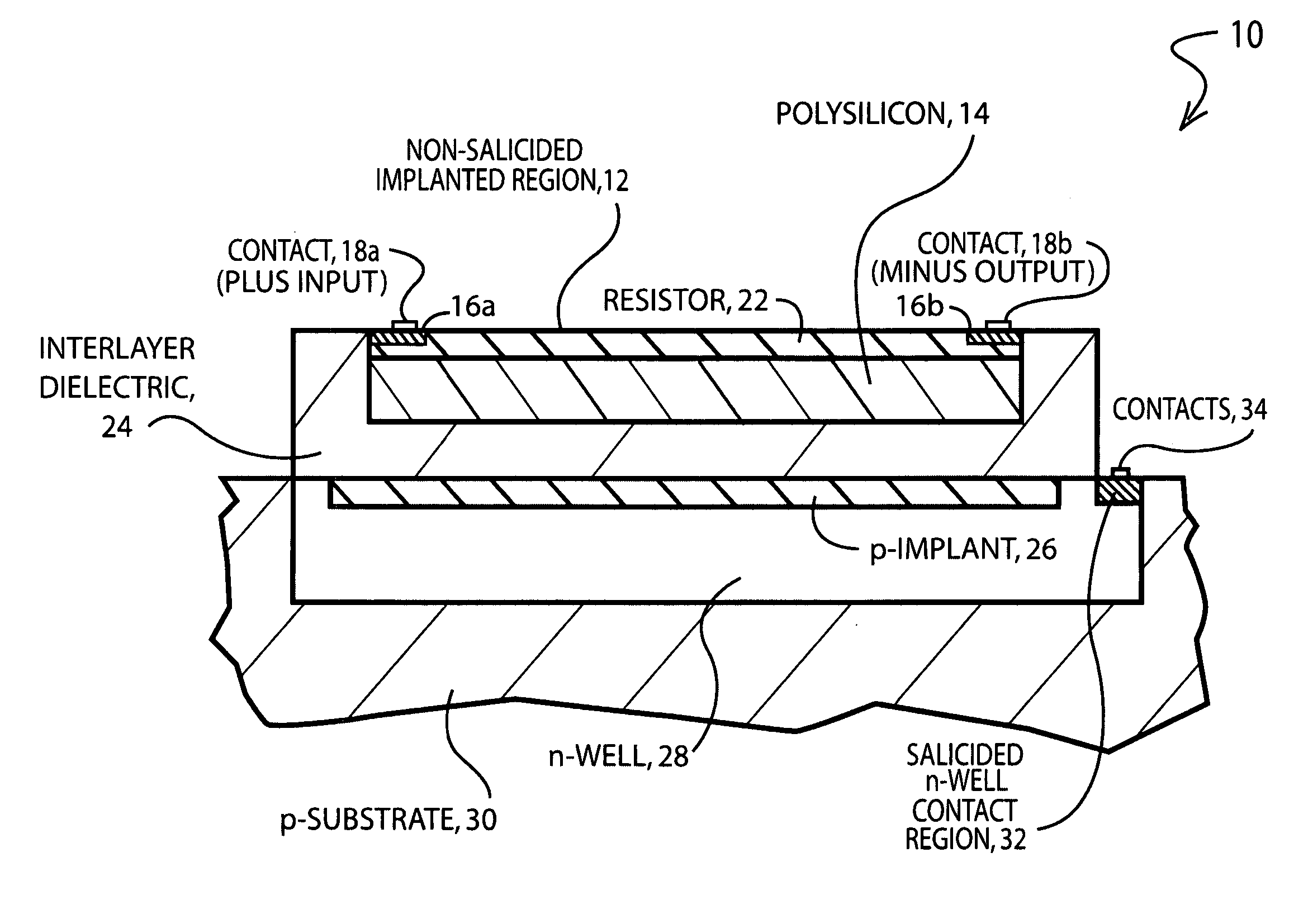
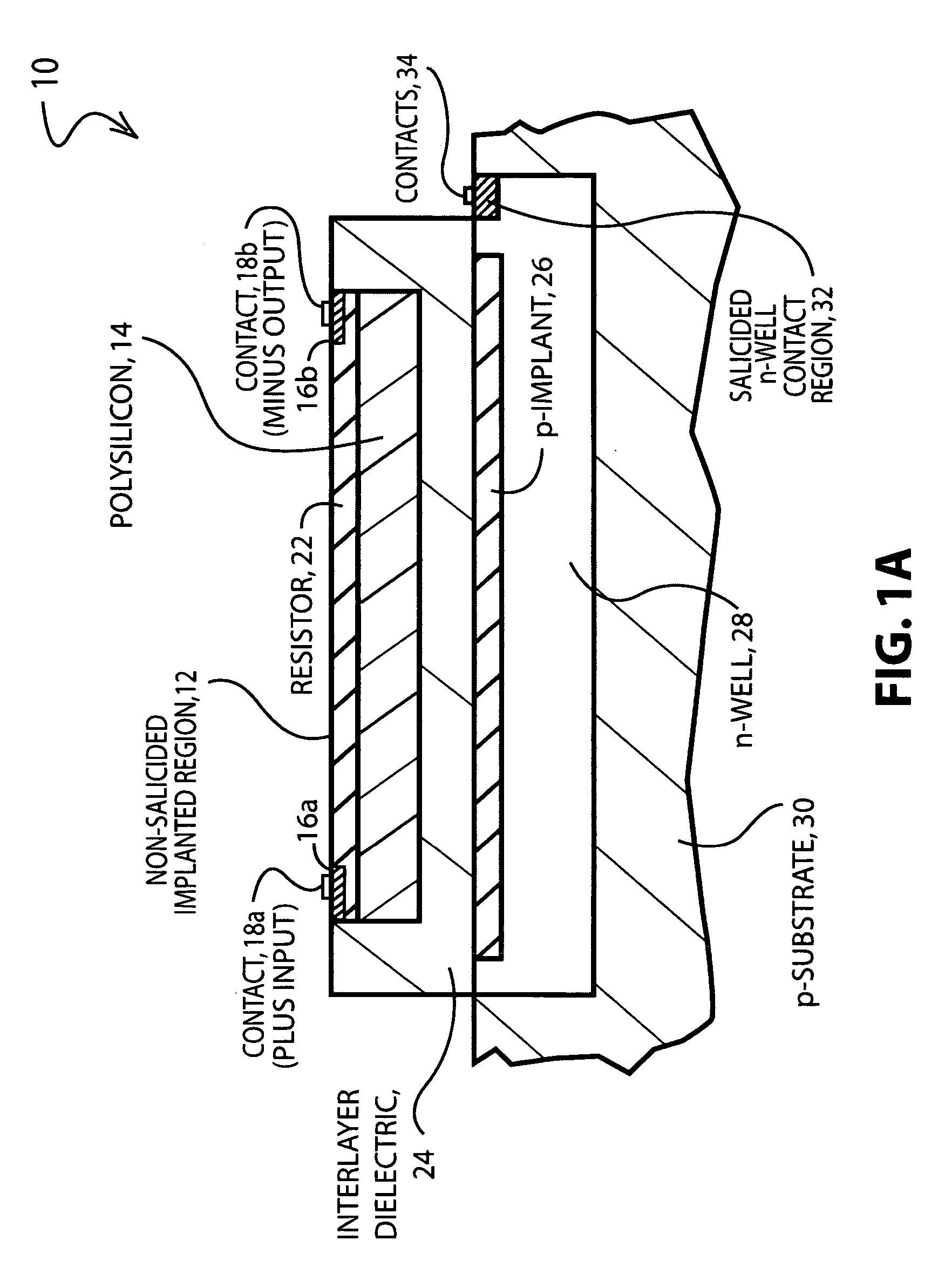
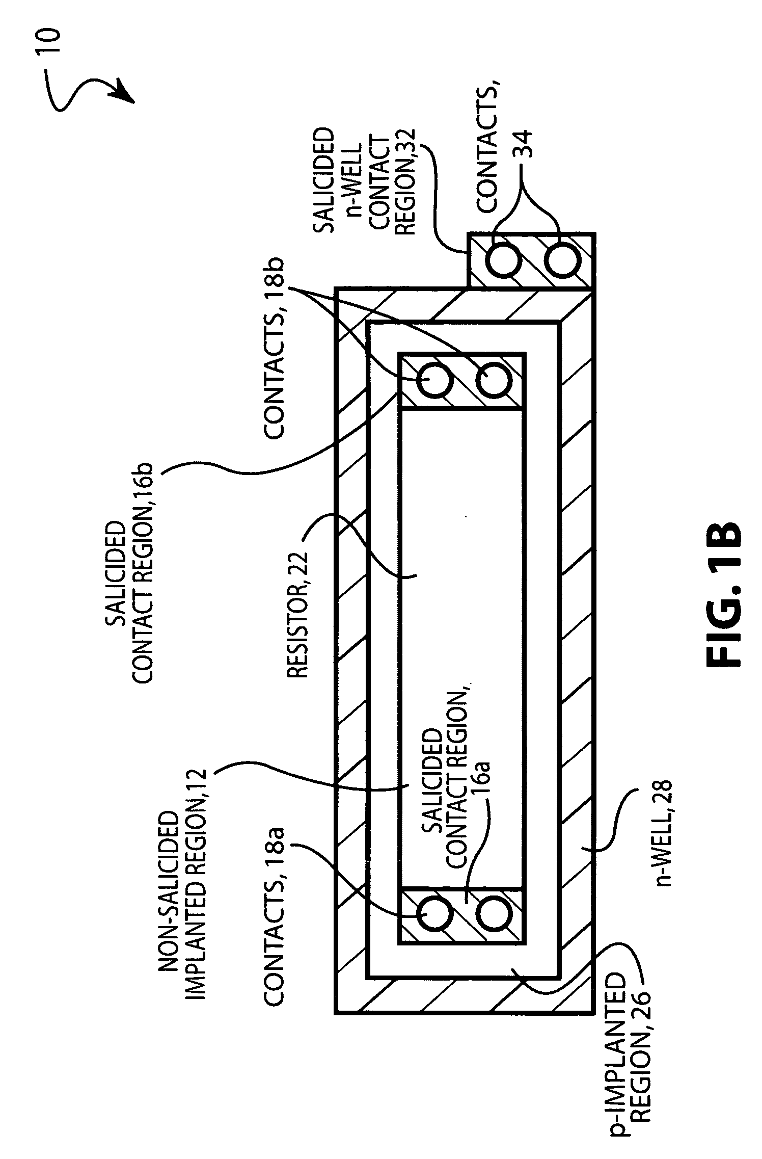
[0015] Briefly, the present invention includes a method for reducing the parasitic capacitance in resistors and resistors embodying this method. A capacitively coupled capacitor is placed in series with the inter-layer dielectric capacitor formed when the resistor is fabricated, by creating a p-type implant inside of an n-well. The depletion region formed thereby generates a series-connected capacitor which reduces the overall capacitance, since capacitors placed in series connection cooperate to reduce the capacitance of the assemblage. The n-well can be placed in electrical connection to ground or connected to a common rail (VDD, for example) to form a reverse biased diode, thereby further increasing the depletion region and reducing the capacitance of the resistor.

[0016] Reference will now be made in detail to the present embodiments of the invention examples of which are illustrated in the accompanying drawings. In what follows, identical callouts will be used for similar or id...


PUM


Abstract

A method for reducing the parasitic capacitance in resistors, and a resistor design embodying this method are described. By creating a p-type or an n-type implant inside of an n-well or a p-substrate, respectively, where the n-well or p-substrate is located in a p-substrate or n-substrate, respectively, a capacitively coupled capacitor is formed in series connection with the parasitic inter-layer dielectric capacitance generated when the resistor is fabricated in the dielectric material. The depletion region formed thereby behaves as a series capacitor which reduces the overall capacitance of the assemblage. The n-well or p-substrate can be placed in electrical connection with a ground potential or brought to a chosen voltage to further increase the depletion region and reduce the capacitance of the resistor.

Description

FIELD OF THE INVENTION [0001] The present invention relates generally to resistors and, more particularly to the reduction of parasitic capacitance for resistors. BACKGROUND OF THE INVENTION [0002] Parasitic capacitance is a problem in resistor manufacturing since this additional capacitance reduces the high-speed response of resistors. The effect is area dependant, and is therefore more pronounced when larger-size resistors are fabricated to minimize resistor matching problems for high-precision analog to digital or digital to analog converters. Use of smaller resistors having improved high-frequency response, leads to poor resistor matching; that is, poor reproducibility of the total resistance value for a set of resistors having the same dimensions. [0003] Accordingly, it is an object of the present invention to provide a resistor having reduced parasitic capacitance. [0004] Another object of the invention is to provide a method for reducing parasitic capacitance in resistors. [0...

Claims


Application Information

Patent Timeline
IPC IPC(8): H01L29/06
CPCH01L27/0802H01L28/20
Inventor ERICKSON, SEAN C.SHAW, JONATHANNUNN, KEVIN R.
Owner BELL SEMICON LLC
Why Eureka
Try Eureka