Method and program for designing semiconductor device

a semiconductor and program technology, applied in the field of method and program for designing a semiconductor device, can solve the problems of not being able to reduce design time, no method for grasping noise value, and much time to improve noise characteristics, so as to reduce the time required and reduce the noise of the power supply

Inactive Publication Date: 2006-06-08
SOCIONEXT INC
View PDF15 Cites 20 Cited by
  • Summary
  • Abstract
  • Description
  • Claims
  • Application Information

AI Technical Summary

Benefits of technology

[0009] The present invention has been developed to eliminate at least one of the above-described problems of the background art, and it is an object of the present invention to provide a semiconductor device design method and program that can rapidly improve power supply noise characteristics even in a large-scaled semiconductor device and that can sufficiently reduce the noise without being restricted in design and noise solution.
[0012] It is thus possible to grasp a value of the power supply noise of the semiconductor device expected to be designed before its circuit is designed through logic synthesis. With this, after making this obtained power supply noise value reflected in setting of the semiconductor device, by making a feedback loop that repeats the step of performing frequency analysis on a power supply distribution network model, the step of performing frequency analysis based on an operating current waveform, and the step of calculating power supply noise, it is possible to obtain various setting values for reduction of the noise value before designing a circuit. By designing the semiconductor device based on the obtained setting values, those setting values can be reflected as restrictions on design, thus making it possible to obtain at an initial stage such a circuit that its power supply noise may fall in a scope of technical standards. Therefore, the feedback loop can be downsized more than a feedback loop that comprises logic synthesis also, thus reducing time required to reduce the power supply noise value can be achieved.

Problems solved by technology

That is, there has been no method for grasping a noise value before the logic synthesis, which is an initial stage of design, nor design flow for considering the noise value before the logic synthesis.
Therefore, feedback to a design parameter of the noise value is made of a large loop in which the logic synthesis, the simulation, and calculation of the noise value are repeated, so that it takes much time to improve noise characteristics, which leads to a problem that design time cannot be reduced.
This leads to an increase in number of work man-hour and hence time required to reduce noise, thus making it impossible to reduce the design time, problematically.
Especially a recent large-scaled semiconductor device requires further more design man-hours, thus making more serious a problem of being unable to reduce the design time.
In the conventional power supply noise-reduction feedback to a completely designed circuit, the circuit once completed is modified, so that as compared to a method of making a modified circuit from the beginning, in this conventional method, the design is somewhat limited and decision conditions are fixed at each stage of the design in many cases.
Therefore, the circuit cannot be changed easily and has fewer solutions, so that noise cannot be reduced enough, leading to a problem of deteriorations in performance of the semiconductor integrated circuit.

Method used


Image

  • Method and program for designing semiconductor device
  • Method and program for designing semiconductor device
  • Method and program for designing semiconductor device

Examples


Embodiment Construction

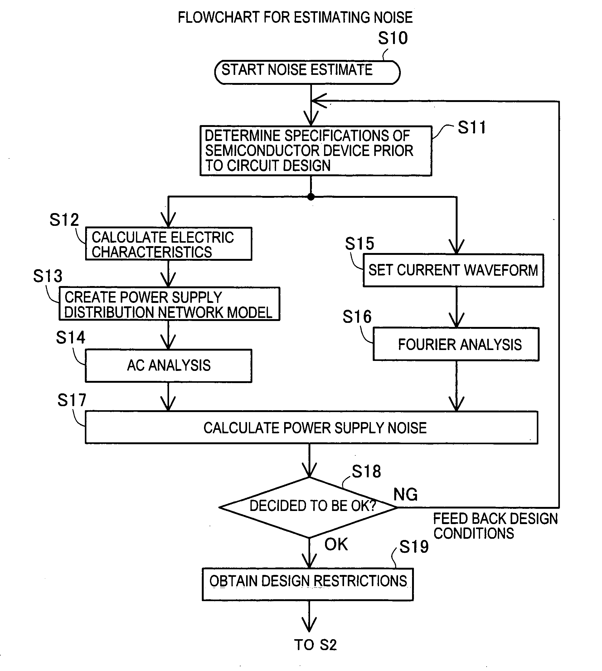
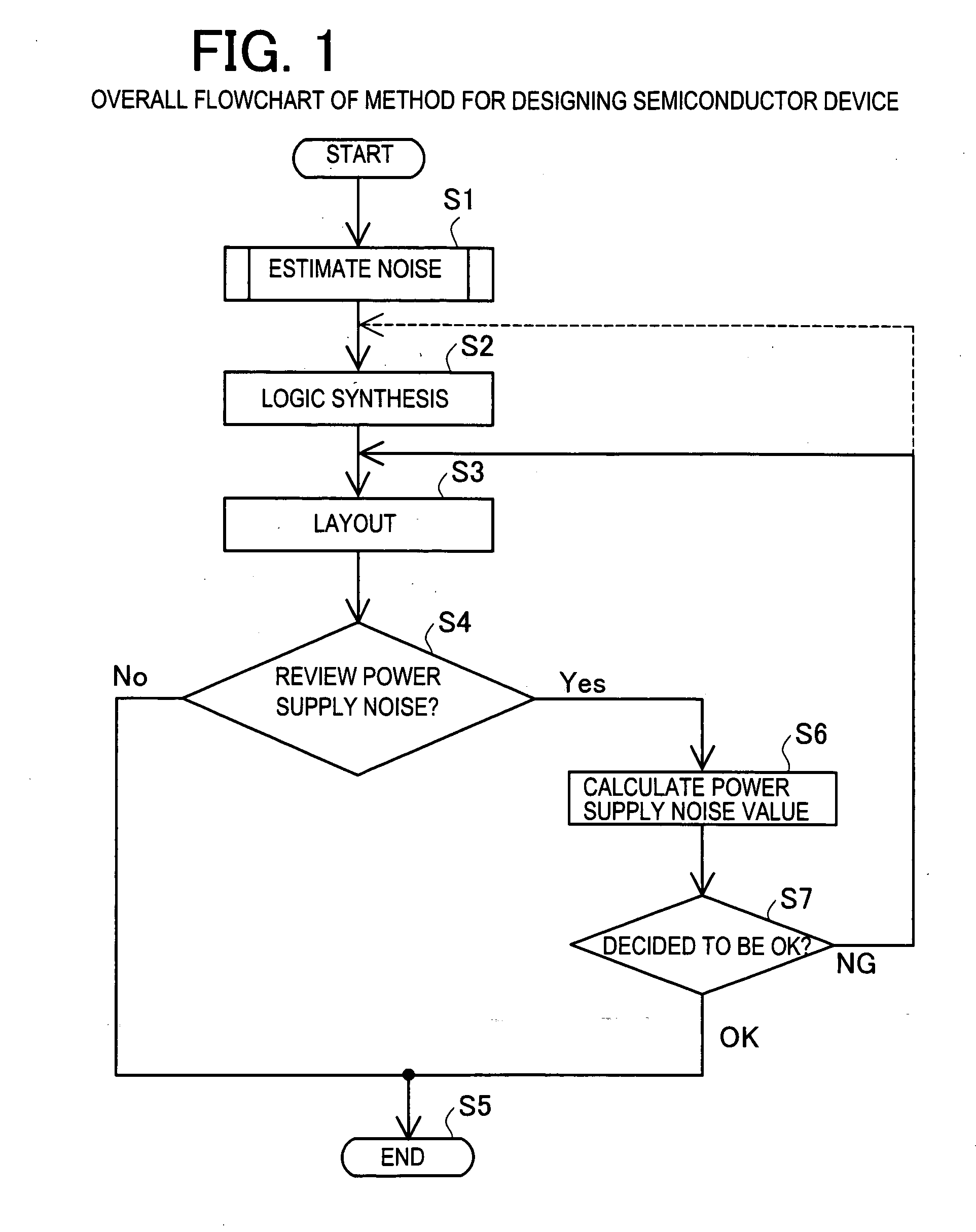
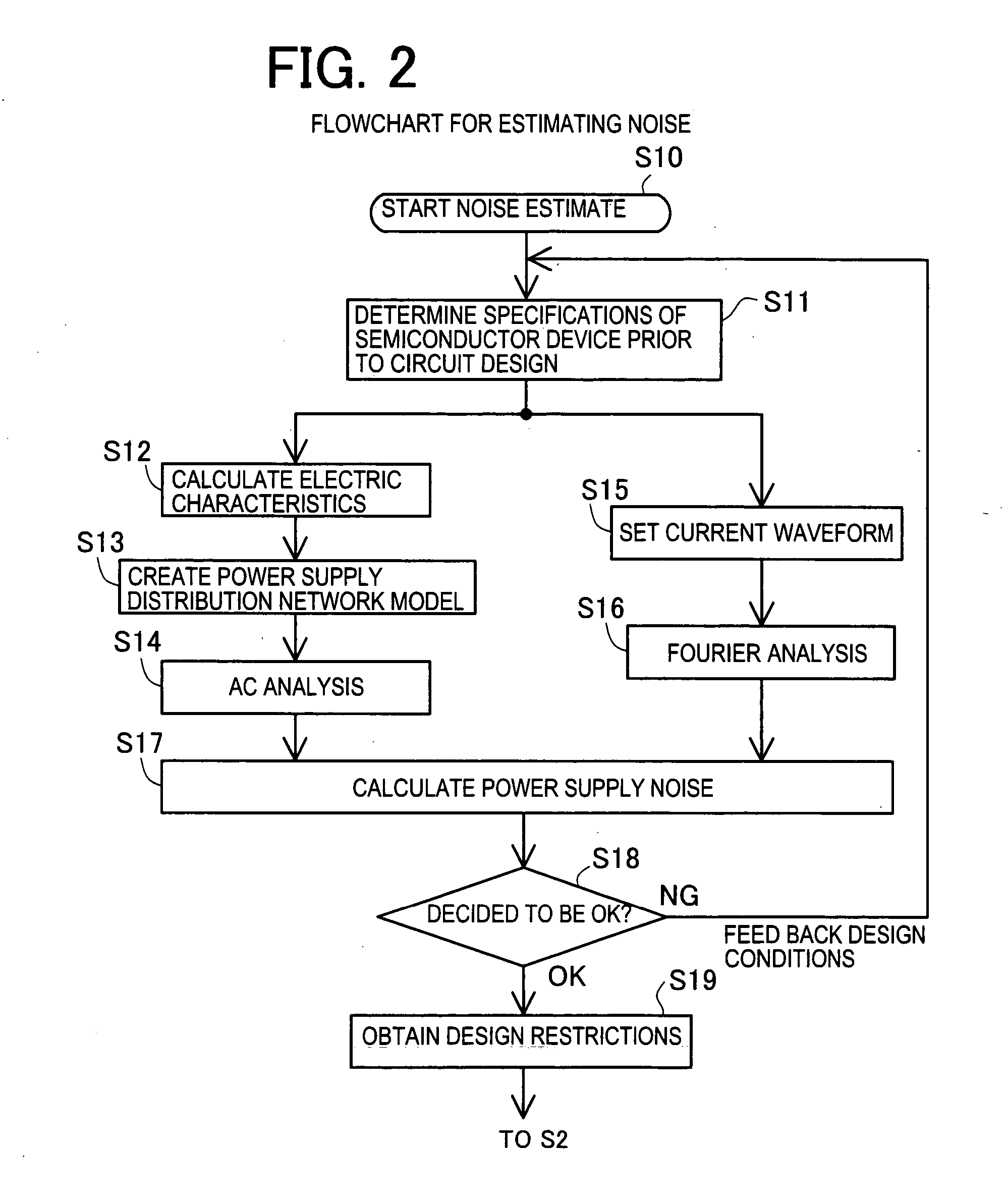
[0027] The following will describe, in detail, preferred embodiments of a semiconductor device design method related to the present invention, with reference to drawings based on FIGS. 1-11. It is to be noted that a concept of the semiconductor device design method contains a semiconductor device manufacturing method. FIG. 1 shows an overall flowchart of the semiconductor device design method related to the present invention. Prior to a circuit design (step 2, hereinafter abbreviated as S2) through logic synthesis and layout (S3), as a pre-stage of starting design, the process estimates a power supply noise value at S1. Contents of S1 are described along a flow of FIG. 2. The flow of FIG. 2 is roughly divided into three steps. From S12 to S14, the process creates a power supply distribution network model that covers from a power supply section of this semiconductor device to a ground potential based on electric characteristics obtained in accordance with specifications of the semico...


PUM


Abstract

It is an object of the present invention to provide a semiconductor device design method and program that can rapidly improve power supply noise characteristics and reduce the noise sufficiently without being restricted in design and noise solution. A step of performing frequency analysis on a power supply distribution network model creates a power supply distribution network model based on electric characteristics obtained in accordance with specifications (maximum allowable drop value of power supply voltage, power supply current value, operating frequency, etc.) of the semiconductor device and performs frequency analysis on this power supply distribution network model. A step of performing frequency analysis based on an operating current waveform analyzes power supply current characteristics based on an operating current waveform obtained in accordance with the specification. A step of calculating power supply noise calculates the power supply noise in accordance with analysis results of the step of performing frequency analysis on the power supply distribution network model and the step of performing frequency analysis based on the operating current waveform. It is thus possible to estimate the power supply noise before designing a circuit of the semiconductor device.

Description

[0001] This application is based upon and claims the benefit of priority from each of the prior Japanese Patent Application No. 2004-349852 filed on Dec. 2, 2004, the entire contents of which are incorporated herein by reference. BACKGROUND OF THE INVENTION [0002] 1. Field of the Invention [0003] The present invention relates to a method and program for designing a semiconductor device and, more particularly to, a method and program that can reduce power supply noise of a semiconductor device. [0004] 2. Description of Related Art [0005] For stable operations of a semiconductor, it is indispensable to design it so that power supply noise may be grasped early and reduced, which is critical especially for a high-speed, large-scale semiconductor in recent years. Work for reduction of a power supply noise value involves feedback to design parameters for the grasping of the noise value and the reduction of the noise. A method for grasping the power supply noise value in a conventional sem...

Claims


Application Information

Patent Timeline
Patent Type & Authority Applications(United States)
IPC IPC(8): G06F17/50G06F9/45
CPCG06F17/5036G06F2217/78Y04S40/22Y02E60/76G06F30/367G06F2119/06Y02E60/00Y04S40/20
Inventor OGAWA, YASUSHIGE
Owner SOCIONEXT INC
Why Eureka
Try Eureka