

Zinc oxide single crystal
a single crystal, zinc oxide technology, applied in the direction of single crystal growth, polycrystalline material growth, chemistry apparatus and processes, etc., can solve the problems of not being difficult natural p type to become p type, and zinc oxide single crystals not suitable for acoustoelectric effect devices, etc., to achieve excellent transparency
- Summary
- Abstract
- Description
- Claims
- Application Information
AI Technical Summary
Benefits of technology
Problems solved by technology
Method used
Image

Examples
examples
[0059] The invention will be explained below in more detail by reference to examples, but the invention should not be construed as being limited to the following examples.
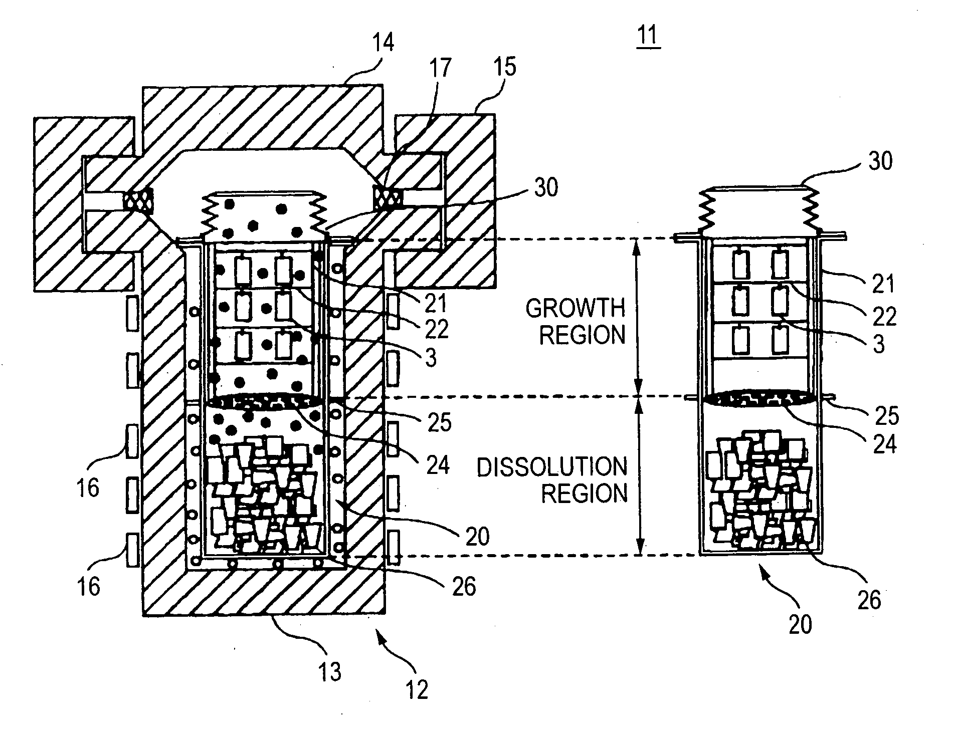
[0060] Using a single crystal growth apparatus having a structure shown in FIG. 1, a ZnO single crystal was grown. The single crystal growth apparatus 11 shown in FIG. 1 comprises an autoclave 12 which can impart its inside with a temperature and a pressure required for growing the ZnO single crystal and a growth chamber 20 housed in the autoclave 12. The autoclave 12 has a structure that, for example, a chamber body 13 of the autoclave 12 formed from a high tension steel containing iron as a main component, is covered via a packing 17 with a lid 14 whose fixation is ensured with a fixing part 15, thereby to airtight—include the inside thereof. A growth chamber 20 used as being housed in the autoclave 12 is made of platinum (Pt) and has a shape approximating a cylinder. On the top, a bellows 30 serving as a pressu...
PUM
 Abstract
Description
Claims
Application Information