Method of estimating substrate temperature

a technology of substrate temperature and temperature, applied in the direction of instruments, heat measurement, thermometer details, etc., can solve the problems of heterostructure device volume production that cannot achieve desired characteristics, rate of growth is susceptible to the temperature of the portion where the reaction proceeds, and the rate of growth is susceptible to the surface temperature of the substra

Inactive Publication Date: 2006-06-15
PANASONIC CORP
View PDF4 Cites 10 Cited by
  • Summary
  • Abstract
  • Description
  • Claims
  • Application Information

AI Technical Summary

Benefits of technology

[0020] With a view to attaining the foregoing objects, the present invention provides a method of estimating substrate temperature comprising the steps of epitaxially growing a first semiconductor layer on a substrate for temperature estimation, the first semiconductor layer being made of a single crystal material having an optical constant that is different from an optical constant of the substrate for temperature estimation, and then epitaxially growing a second semiconductor layer on the first semiconductor layer under a reaction control condition, the second semiconductor layer being made of a single crystal material having an optical constant that is substantially equal to the optical constant of the substrate for temperature estimation and different from the optical constant of the first semiconductor layer; measuring a film thickness of the second semiconductor layer by a method of optical measurement while measuring a surface temperature of the second semiconductor layer; calculating a rate of growth of the second semiconductor layer based on the film thickness of the second semiconductor layer thus measured to derive a relationship between the rate of growth of the second semiconductor laye

Problems solved by technology

This is because, without such control, volume production of heterostructure devices exhibiting desired characteristics would be impossible.
The CVD process causes epitaxial growth to proceed by the chemical reaction between the material of the substrate on the substrate surface and the source material molecule as described above and, hence, the rate of growth is susceptible to the temperature of the portion where reaction proceeds.
In the case of the UHV-CVD (Ultra High Vacuum Chemical Vapor Deposition) process employed for epitaxial growth of an SiGe mixed crystal, in particular, the rate of growth is susceptible to the surface temperature of the substrate.
This is because even if the growth conditions other than the substrate temperature, such as the gas flow rate and growth time are reproduced precisely, a failure to reproduce the substrate temperature results in a grown layer having a film thickness and a composition ratio profile that are different from desired ones, thus making it impossible to fabricate heterostructure devices having desired characteristics.
That is, if the temperature distribution in the plane of a substrate under epitaxial growth cannot be determined, adjustment to make the temperature in the plane of the substrate uniform is impossible.
Further, if the temperatures of respective substrates cannot be measured, it is impossible to reproduce a desired substrate surface temperature.
However, the thermocouple needs to be placed close to a subject of measurement, i.e. a substrate surface because of its

Method used


Image

  • Method of estimating substrate temperature
  • Method of estimating substrate temperature
  • Method of estimating substrate temperature

Examples


embodiment 1

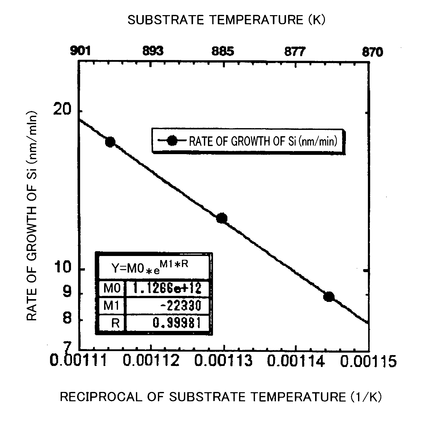
[0043] The following description is directed to a method of estimating substrate temperature according to the present invention utilized in the fabrication of an HBT as one of heterostructure devices. For easy understanding, the structure of and the fabrication process for an HBT having a SiGe mixed crystal film (hereinafter referred to as “SiGeHBT”) will be described first.

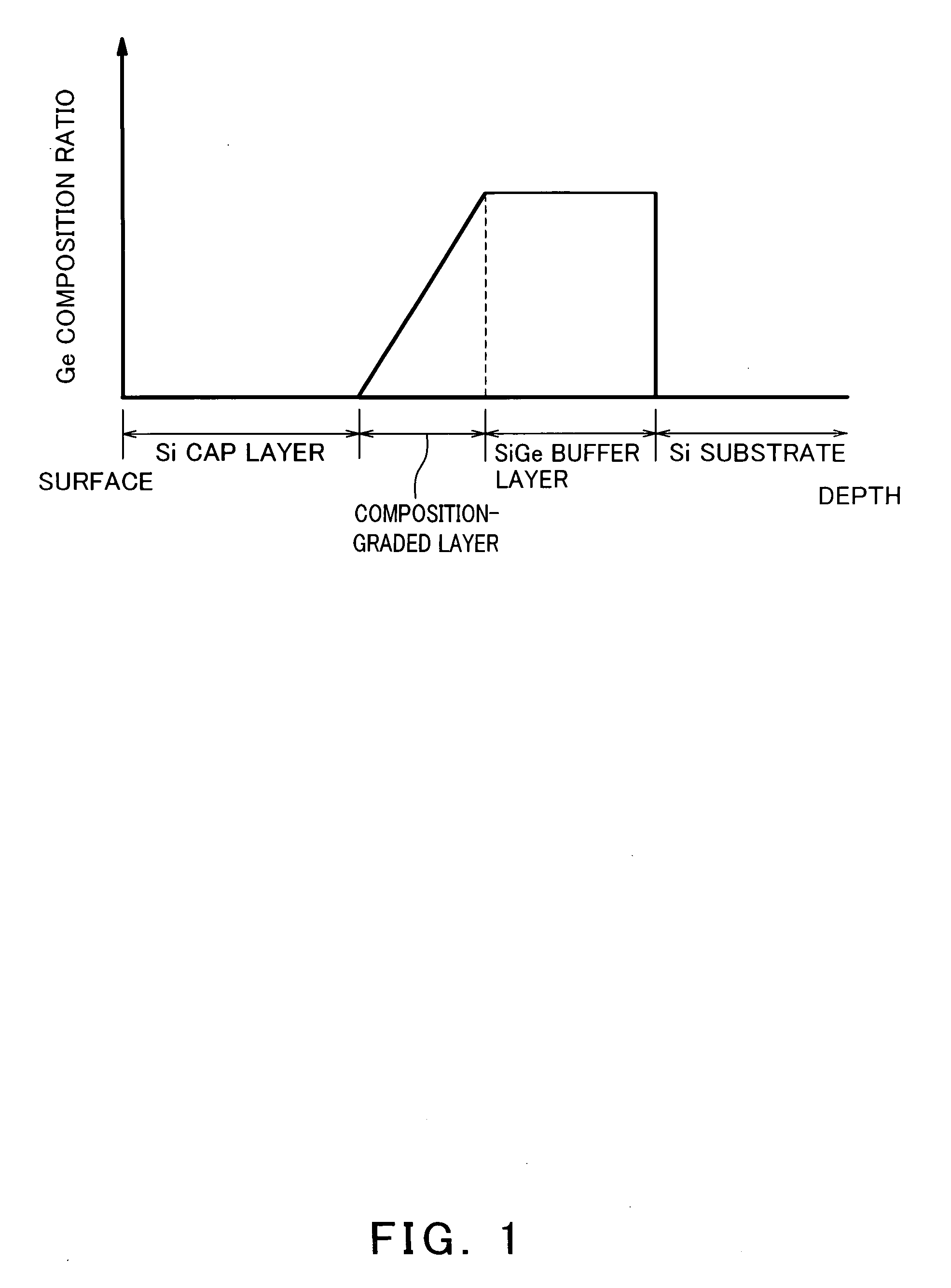
[0044]FIG. 1 is a diagram showing a graph of a Ge composition ratio profile in the SiGeHBT. In FIG. 1, the ordinate axis indicates Ge composition ratio while the abscissa axis indicates depth from the surface of a semiconductor layer stacked on a Si substrate.

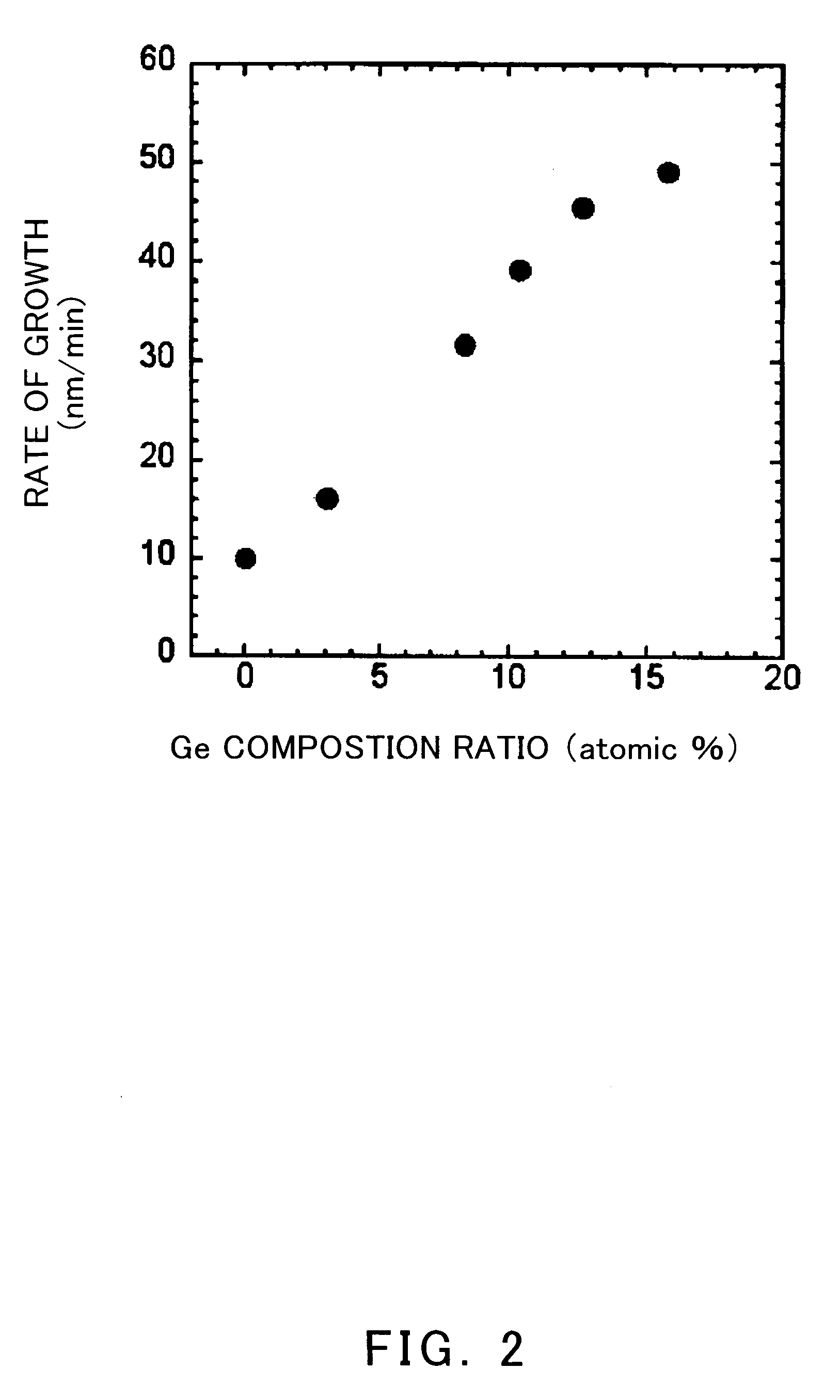
[0045] As shown in FIG. 1, the SiGeHBT is constructed by sequentially stacking a SiGe buffer layer having an invariant Ge composition ratio, a B-doped, composition-graded layer having decreasing Ge composition ratio as it is closer to the surface and a Ge-free Si cap layer on a Si substrate provided with a pattern.

[0046] Such a structure having varying Ge...

embodiment 2

[0097] In embodiment 1, the substrate temperature of the substrate for device fabrication and the rate of growth of the growing layer in the second structure are measured at one point. In embodiment 2, on the other hand, the substrate temperature of the substrate for device fabrication and the rate of growth of the growing layer in the second structure are measured at plural points. By so doing, it is possible to know the distribution of substrate temperature in the plane of the substrate for device fabrication.

[0098] First, the first stage of embodiment 1 is carried out. Subsequently, the second stage of embodiment 1 is carried out to form a second structure and the film thickness of a Si-containing layer is measured with a spectroscopic ellipsometer or spectral reflectometer. The spectroscopic ellipsometer or spectral reflectometer used in this embodiment has a movable stage on which the second structure is placed and hence is capable of measuring the film thickness of the Si-con...


PUM


Abstract

A method of estimating substrate temperature according to this invention includes the steps of epitaxially growing a Si-containing layer (103) on a SiGe layer (102) formed on a substrate for temperature estimation (101) constituted of a Si substrate under a reaction control condition; finding a relationship between a rate of growth of the Si-containing layer and a substrate temperature of the substrate for temperature estimation; epitaxially growing a Si-containing layer on a substrate for device fabrication as a subject of substrate temperature estimation under a reaction control condition; and estimating a substrate temperature of the substrate for device fabrication based on the rate of growth of the latter Si-containing layer and the relationship between the rate of growth of the former Si-containing layer (103) and the substrate temperature of the substrate for temperature estimation.

Description

[0001] This is a continuation application under 35 U.S.C.111(a) of pending prior International Application No. PCT / JP02 / 11250, filed on Oct. 30, 2002. BACKGROUND OF THE INVENTION [0002] 1. Field of the Invention [0003] The present invention relates to a method of estimating a surface temperature of a substrate during epitaxial growth of a semiconductor layer on the substrate in a semiconductor device fabrication process. [0004] 2. Description of the Related Art [0005] In recent years, there have been developed high-performance semiconductor devices so-called heterostructure devices such as hetero bipolar transistors (hereinafter referred to as “HBTs”). Such a heterostructure device is fabricated by epitaxial growth of a crystal that is different from the substrate. The use of such epitaxial growth technology makes it possible to stack thin crystal films that are different in physical properties from each other with a high precision of the order of about a mono atomic layer to severa...

Claims


Application Information

Patent Timeline
IPC IPC(8): G01K13/00
CPCG01K11/02Y10S438/933
Inventor NOZAWA, KATSUYASAITOH, TOHRUOHNISHI, TERUHITO
Owner PANASONIC CORP
Why Eureka
Try Eureka