
Method and apparatus for clamping a substrate in a high pressure processing system

Inactive Publication Date: 2006-06-22
TOKYO ELECTRON LTD
View PDF99 Cites 7 Cited by
  • Summary
  • Abstract
  • Description
  • Claims
  • Application Information

AI Technical Summary

Benefits of technology

[0015] An objective of the present invention is to provide a pressure biased wafer holder for a high pressure processing system, and a system and method for pressure biased wafer holding in high pressure processing systems. A further objective of the invention is to provide a high pressure processing system and wafer holder therefor that overcomes the problems of the prior art. A more particular objective of the present invention is to provide a vacuum chuck for a high pressure processing system, for example a supercritical fluid processing system, that will avoid platen deformation and other problems of high pressure processing of substrates, for example, of semiconductor wafers.
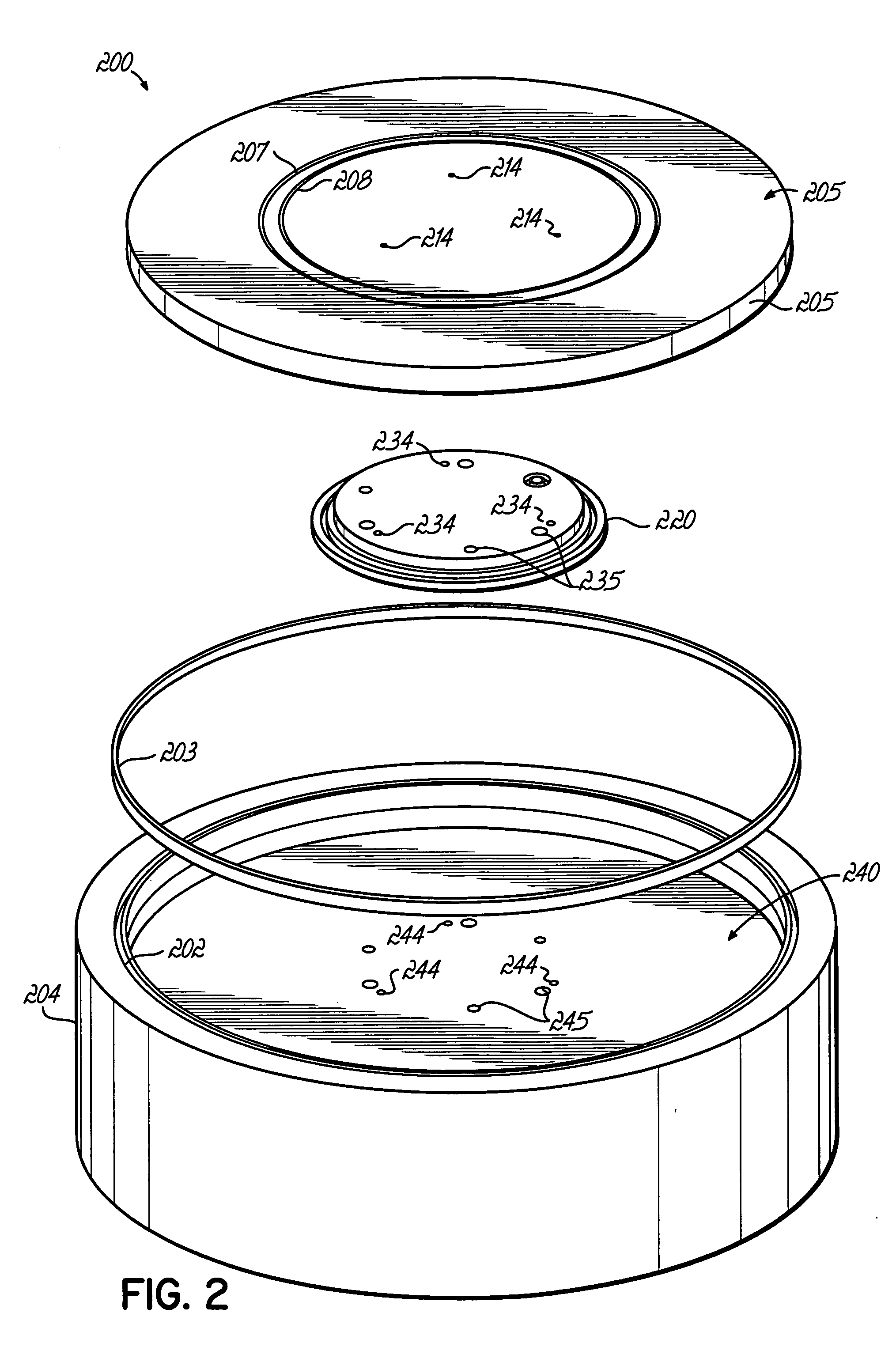
[0017] According to certain embodiments of the present invention, a wafer holder is provided for holding a semiconductor wafer by fluid pressure bias when processing the wafer in a processing chamber with a high pressure fluid. The wafer holder includes a platen disk having a wafer supporting surface on its frontside and passages therein that communicate with the wafer supporting surface and located to apply relatively low pressure to the backside of a wafer supported on the wafer supporting surface to hold the wafer to the platen from the pressure of the high pressure fluid. A rigid pressure plate holds the disk in a cavity that is configured to receive the platen disk while forming a gap between the disk and the pressure plate to communicate high pressure fluid behind the disk to substantially isolate the platen disk from a substantial pressure gradient between its front and back sides.

Problems solved by technology

Moreover, the advent of new materials, such as low dielectric constant (low-k) materials, limits the use of plasma ashing due to their susceptibility to damage during plasma exposure.
Certain challenges occur when attempting to process silicon wafers under high pressure.
One such issue is how to hold the wafer in place during processing.
In such a case, bias in pressure keeps the wafer in place during processing, which may include violent events such as sudden decompressions, high surface velocity jets for cleaning, etc.
One of the significant drawbacks of vacuum holding is the restraining of the wafer against the platen.
If a wafer is held against a platen, typically of stainless steel, the resulting static pressure load can force the wafer against the platen, which can cause damage to the backside of the wafer.
This can cause irreparable harm to the wafer for subsequent process steps.
The wafer may or may not be able to follow the new shape that the platen is forced into due to the pressure load.
Results of this flexing can break wafers, because they are brittle and fragile and cannot elastically deform like stainless steel.
It can also cause a grinding or fretting effect between the wafer and the platen, due to the high forces and small displacements which take place.
This can create metal or silicon particles to be interspersed between the wafer and platen, which in turn can damage the current wafer, and be present on the platen to damage subsequent wafers that are processed.
The magnitude of this flexing may be considered trivial under ordinary industrial circumstances.
Unfortunately with semiconductor wafers, flexing of less than 0.0010 inches, or even as little as 0.0005 inches, have been shown to cause significant damage to wafers, or wafer breakage.
Misalignment of features on the wafer platen, or poor flatness of the platen surface can also result in wafer breakage if the holding load is high.

Method used


Image

  • Method and apparatus for clamping a substrate in a high pressure processing system
  • Method and apparatus for clamping a substrate in a high pressure processing system
  • Method and apparatus for clamping a substrate in a high pressure processing system

Examples


Embodiment Construction

[0029] In the following description, to facilitate a thorough understanding of the invention and for purposes of explanation and not limitation, specific details are set forth, such as a particular geometry of the processing system and various descriptions of the system components. However, it should be understood that the invention may be practiced with other embodiments that depart from these specific details.

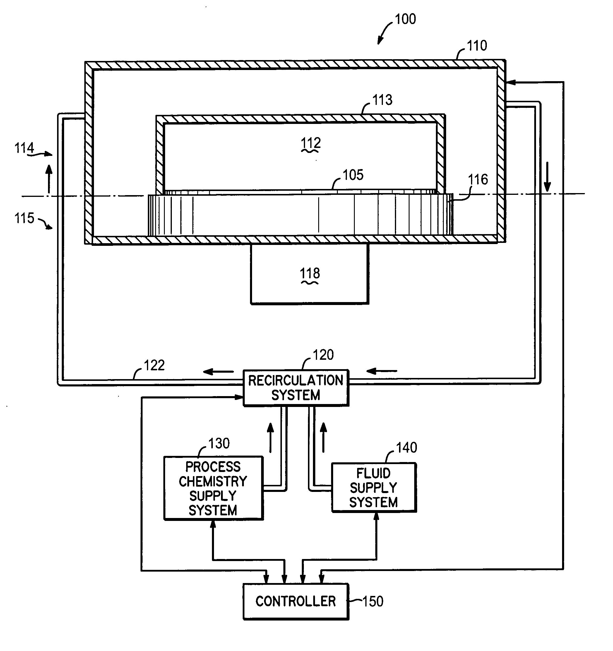
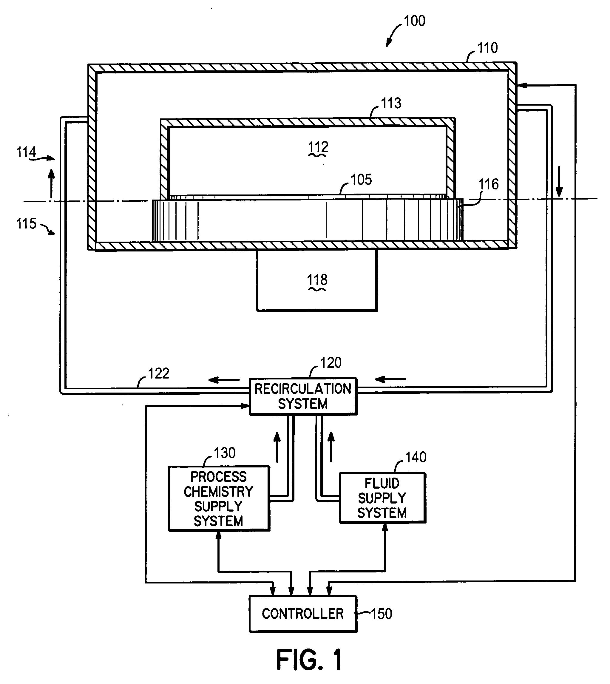
[0030] Referring now to the drawings, wherein like reference numerals designate identical or corresponding parts throughout the several views, FIG. 1 illustrates a processing system 100 according to an embodiment of the invention. In the illustrated embodiment, processing system 100 is configured to treat a substrate 105 with a high pressure fluid, such as a fluid in a supercritical state, with or without other additives, such as process chemistry. The processing system 100 comprises processing elements that include a processing chamber 110, a fluid flow system 120, a proces...


PUM

PropertyMeasurementUnit
Thicknessaaaaaaaaaa
Thicknessaaaaaaaaaa
Diameteraaaaaaaaaa

Abstract

An isolated semiconductor wafer platen is disclosed for use in high pressure processing. The use of vacuum chucking for holding a semiconductor wafer during processing is well known in the art and can be applied to high pressure systems as well, but some difficulties can arise under high pressure processes. Small deflections in even very thick metal support platens can lead to backside wafer wear, platen abrasion, and even breakage of semiconductor wafers. This invention discloses a method to eliminate the transfer of flexure inherent in high pressure vessel walls, yet still retain the vacuum chucking method.

Description

FIELD OF THE INVENTION [0001] The present invention relates to a method and system for clamping a substrate in a high pressure processing system and, more particularly, in a supercritical processing system. BACKGROUND OF THE INVENTION [0002] During the fabrication of semiconductor devices for integrated circuits (ICs), a sequence of material processing steps, including both pattern etching and deposition processes, are performed, whereby material is removed from or added to a substrate surface, respectively. During, for instance, pattern etching, a pattern formed in a mask layer. of radiation-sensitive material, such as photoresist, using for example photolithography, is transferred to an underlying thin material film using a combination of physical and chemical processes to facilitate the selective removal of the underlying material film relative to the mask layer. [0003] Thereafter, the remaining radiation-sensitive material, or photoresist, and post-etch residue, such as hardened...

Claims


Application Information

Patent Timeline
IPC IPC(8): B08B7/04
CPCH01L21/6838Y10S134/902
Inventor SHEYDAYI, ALEXEI
Owner TOKYO ELECTRON LTD
Learn More