Optical-routing boards for opto-electrical systems and methods and apparatuses for manufacturing the same

Inactive Publication Date: 2006-06-22
FUJITSU LTD
View PDF3 Cites 22 Cited by
  • Summary
  • Abstract
  • Description
  • Claims
  • Application Information

AI Technical Summary

Benefits of technology

[0012] It is another object of the present invention to enable the creation of long, low-loss optical waveguides in optical interconnect boards for electronic systems and the like.
[0013] It is another object of the present invention to enable the formation of a high-density of waveg

Problems solved by technology

As high-end computers increase in complexity and chip count, the interconnections between IC chips have grown and bottleneck delays for these interconnections have increased.
However, the polymer materials for these layers have anisotropic dielectric constants, and thus have high degrees of birefringence.
The birefringence hinders the transmission of signals in the waveguides by causing spatial and temporal dispersion of optical signals, an

Method used


Image

  • Optical-routing boards for opto-electrical systems and methods and apparatuses for manufacturing the same
  • Optical-routing boards for opto-electrical systems and methods and apparatuses for manufacturing the same
  • Optical-routing boards for opto-electrical systems and methods and apparatuses for manufacturing the same

Examples


Example

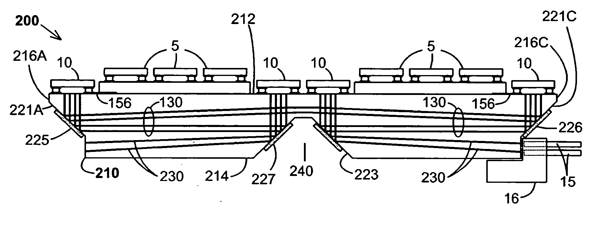
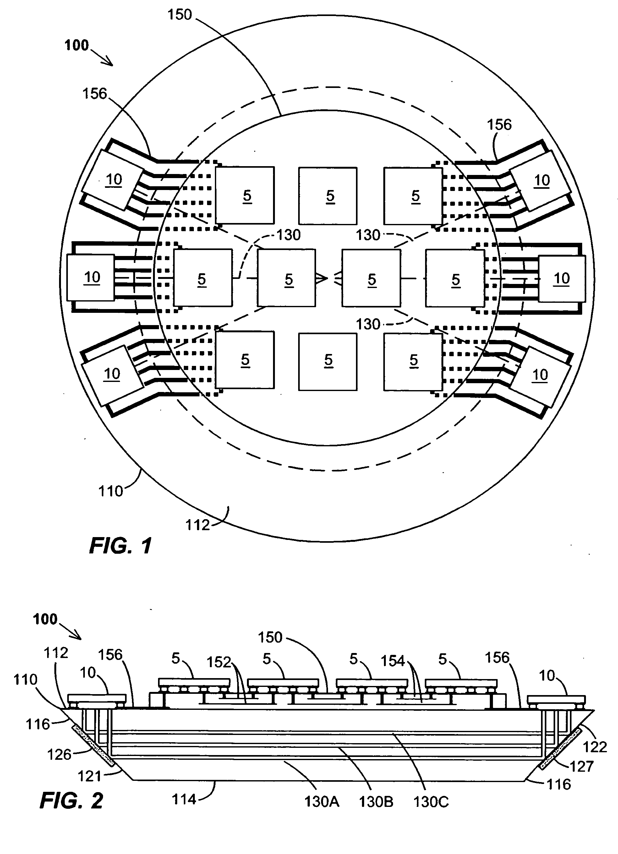
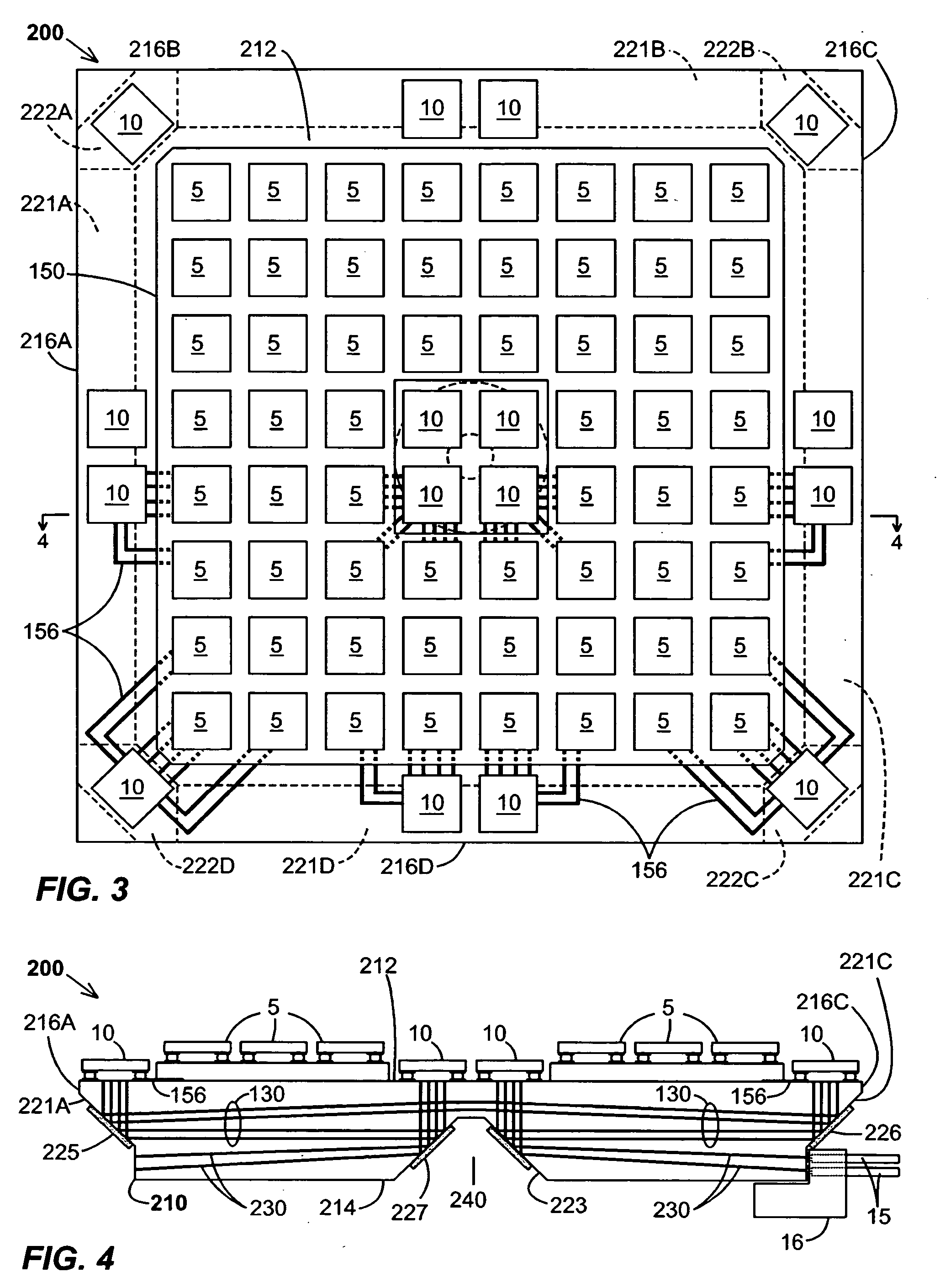
[0025] A top plan view of a first optical-routing board 100 is shown in FIG. 1, and a cross-sectional view thereof is shown in FIG. 2. Referring to FIG. 1, optical-routing board 100 is for holding a plurality of IC chips 5 disposed in the central area of board 100, and a plurality of opto-electric chips 10 disposed around the periphery of board 100. For visual simplicity, ten IC chips 10 and six opto-electric chips 5 are shown in FIG. 1. In typical applications, there may be tens to hundreds of IC chips 5, and tens of opto-electric chips 10, with the diameter of board 100 being relatively large (e.g., 20 cm to 40 cm). Referring to both FIGS. 1 and 2, optical-routing board 100 comprises a substrate 110 having a top surface 112, a bottom surface 114, and one or more sides 116. Selected IC chips 5, usually those closest to the side(s) 116, are electrically coupled to opto-electric chips 10 by a plurality of electrical traces 156 formed on the substrate's top surface 112. In addition, a...


PUM


Abstract

Disclosed are optical-routing boards for opto-electrical systems having optical waveguides embedded in non-laminated optical substrates that enable optical signals to be routed among opto-electric components mounted on the top surfaces of the optical substrates. Methods for making the optical-routing boards are also disclosed. The waveguides are formed by focused pulse-laser writing, with the focal point of the pulsed-laser beam being moved in a three-dimensional manner through the non-laminated substrate. Bevel surfaces are preferably formed in the substrate to facilitate bending of the waveguides.

Description

FIELD OF THE INVENTION [0001] The present invention relates to boards for opto-electrical systems, and more particularly to boards having embedded optical waveguides that enable optical signals to be routed among opto-electric components mounted on the substrate. BACKGROUND OF THE INVENTION [0002] As high-end computers increase in complexity and chip count, the interconnections between IC chips have grown and bottleneck delays for these interconnections have increased. There have been many efforts to address the bottleneck delays by conveying some of the signals between chips by optical means. In these attempts, bottlenecked electrical signals are converted to optical signals by light transmitters, the optical signals are then propagated over long distances across an interconnect board by way of optical waveguides formed therein, and then received by light receivers and converted back to electrical signals. The optical waveguides in these boards are typically formed by polymer layer...

Claims


Application Information

Patent Timeline
IPC IPC(8): G02B6/12
CPCG02B6/43H05K1/0274
Inventor LIU, KUO-CHUAN
Owner FUJITSU LTD
Why Eureka
Try Eureka