Method to improve device isolation via fabrication of deeper shallow trench isolation regions

Inactive Publication Date: 2006-06-22
CHARTERED SEMICONDUCTOR MANUFACTURING
View PDF11 Cites 40 Cited by
  • Summary
  • Abstract
  • Description
  • Claims
  • Application Information

AI Technical Summary

Benefits of technology

[0008] It is still another object of this invention to form a silicon oxide region at the bottom portion of the shallow trench shape prior t

Problems solved by technology

The more robust dry etch procedure can however lead to defect generation in adjacent semiconductor regions.
In addition deeper and narr

Method used


Image

  • Method to improve device isolation via fabrication of deeper shallow trench isolation regions
  • Method to improve device isolation via fabrication of deeper shallow trench isolation regions
  • Method to improve device isolation via fabrication of deeper shallow trench isolation regions

Examples


Example

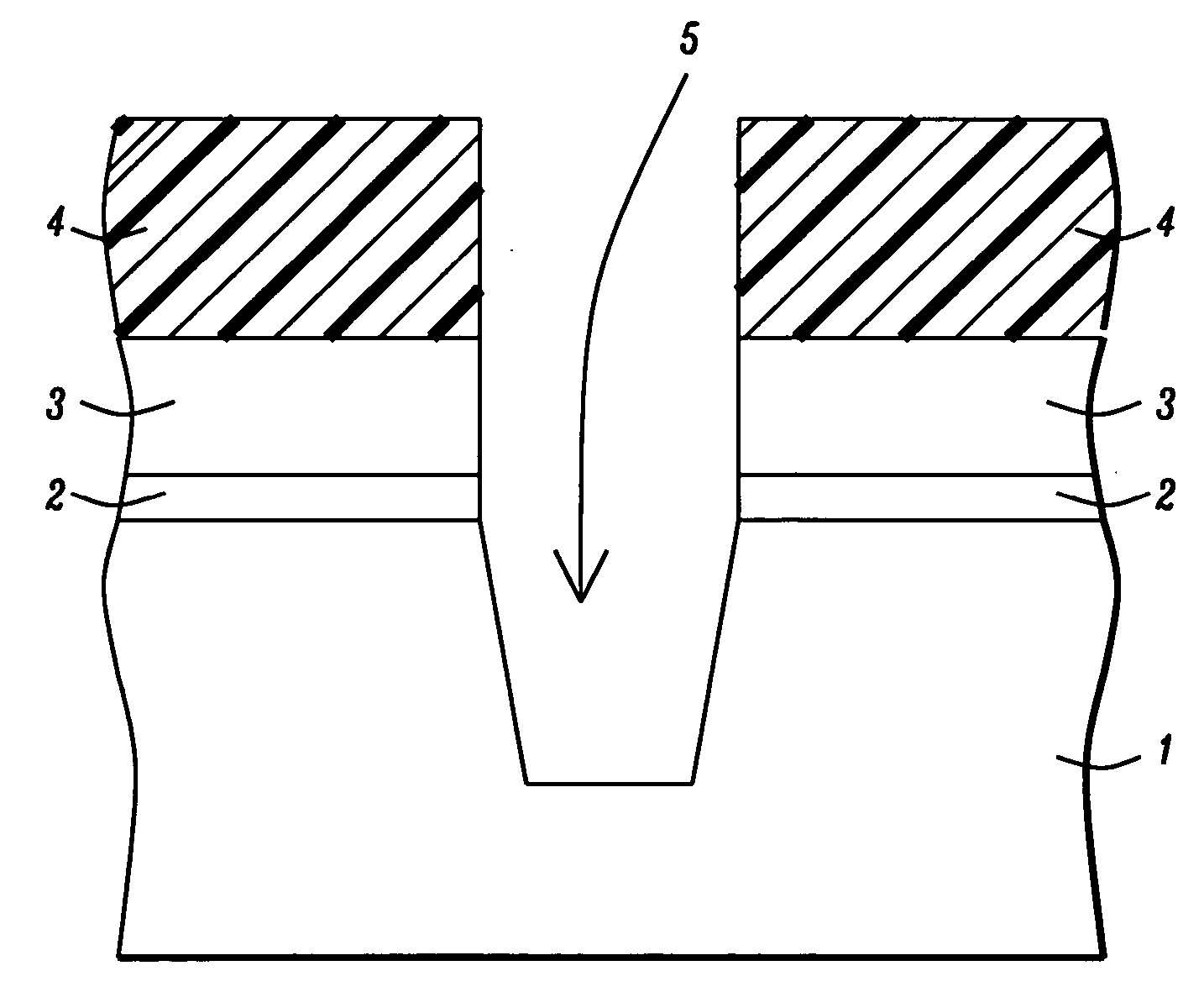
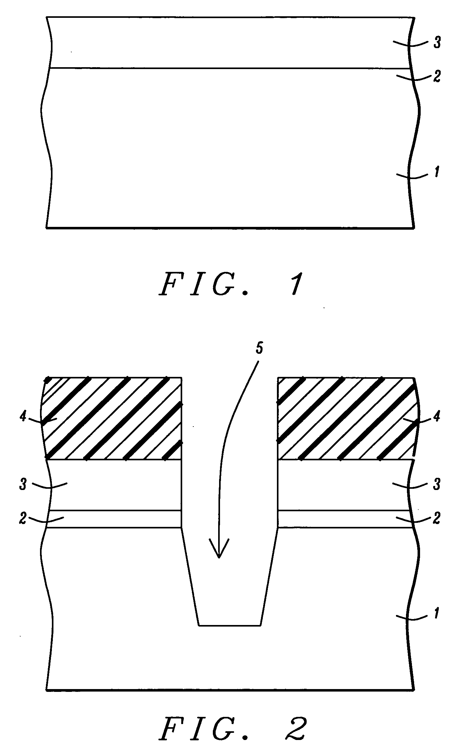
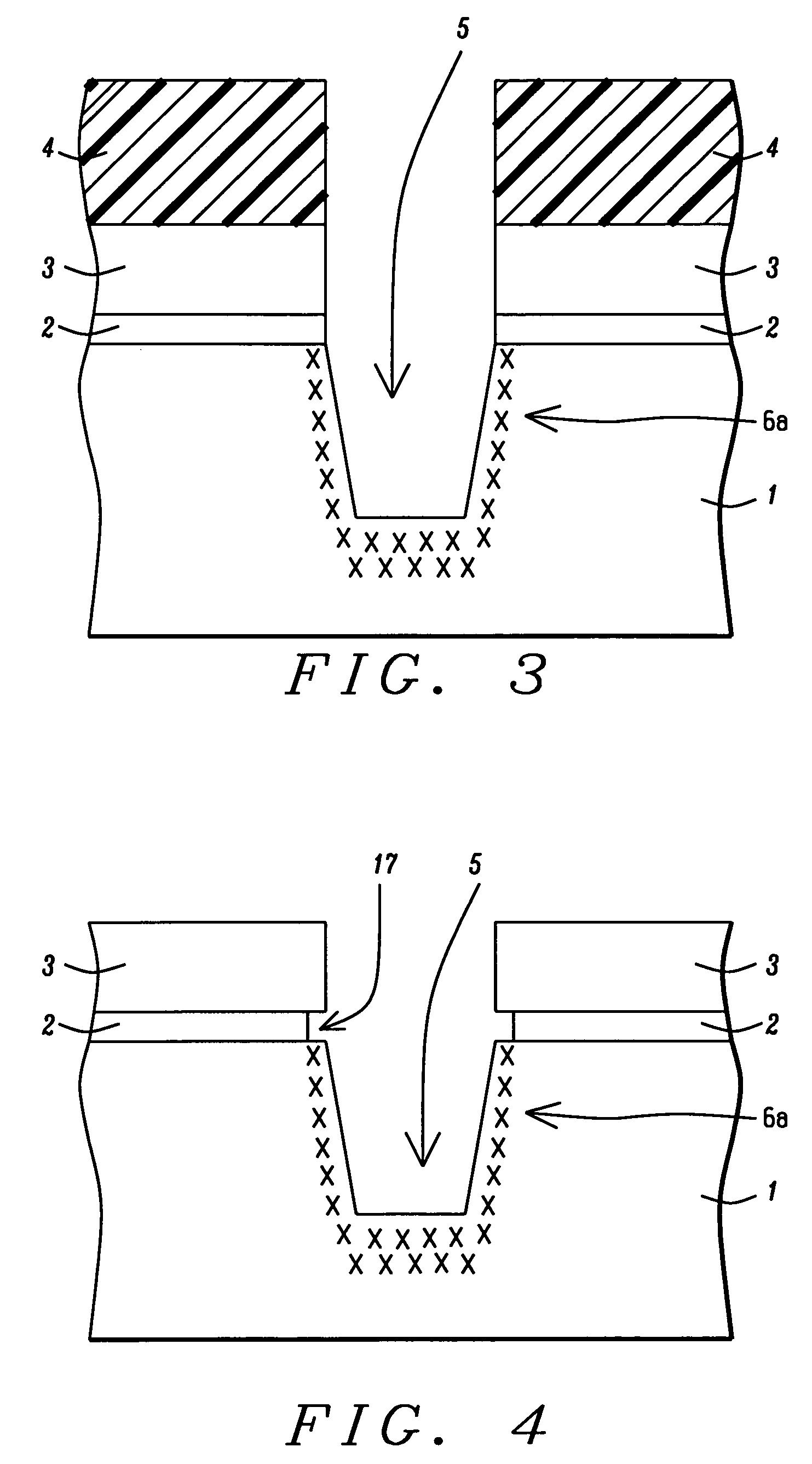
[0012] The method of forming an STI structure wherein the depth of the insulator filled STI structure is extended with a silicon oxide region formed below a pre-insulator filled STI shape via a self aligned oxygen implantation and anneal procedure, will now be described in detail. Semiconductor substrate 1, comprised of single crystalline silicon featuring a crystallographic orientation, is shown schematically in FIG. 1. Silicon oxide layer 2, either thermally grown, or obtained via low pressure chemical vapor deposition (LPCVD) or plasma enhanced chemical vapor deposition (PECVD) procedures at a thickness between about 80 to 120 Angstroms, is next formed on semiconductor substrate 1. Silicon nitride layer 3, at a thickness between about 1400 to 1800 Angstroms, is now deposited via LPCVD or PECVD procedures.

[0013] Photoresist shape 4, is next formed with a defined opening between about 0.2 to 1.0 micrometers (um), exposing a portion of the top surface of silicon nitride layer 3. A...


PUM


Abstract

A method of forming a shallow trench isolation (STI) structure wherein the depth of the STI structure has been extended via formation of an underlying silicon oxide region, has been developed. After definition of a shallow trench isolation shape in a top portion of a semiconductor substrate a self-aligned ion implantation procedure is employed to place oxygen ions in portions of the semiconductor substrate exposed at the bottom portion of the shallow trench shape. Growth of a liner layer on the exposed surfaces of the shallow trench shape, or growth of a liner layer followed by anneal procedure, results in activation of the implanted oxygen ions creating the desired silicon oxide region in a portion of the semiconductor substrate underlying the bottom of the shallow trench shape. Insulator filling of the shallow trench shape now results in a deeper STI structure comprised of the insulator filled shallow trench shape and the underlying silicon oxide region.

Description

BACKGROUND OF THE INVENTION [0001] (1) Field of the Invention [0002] The present invention relates to methods used to fabricate semiconductor devices and more specifically to a method used to increase the depth of a shallow trench isolation (STI) region without increasing the depth of a shallow trench shape. [0003] (2) Description of Prior Art [0004] Isolation between semiconductor devices as well as between specific elements of semiconductor devices has been accomplished via shallow trench isolation structures comprised of insulator filled, shallow trench shapes. Increased STI depth allows greater reductions of device leakage current and of device noise cross-talk to be realized while also allowing increased device latch up performance to occur. One method of increasing STI depth, and thus enhanced device performance, is the fabrication of deeper STI shapes in a semiconductor substrate achieved via longer dry etching procedures. The more robust dry etch procedure can however lead t...

Claims


Application Information

Patent Timeline
IPC IPC(8): H01L21/76
CPCH01L21/76235H01L21/76237H01L21/26506
Inventor ZHANG, GUOWEI
Owner CHARTERED SEMICONDUCTOR MANUFACTURING
Why Eureka
Try Eureka