Novel combo memory design and technology for multiple-function java card, sim-card, bio-passport and bio-id card applications

Active Publication Date: 2006-06-29
CALLAHAN CELLULAR L L C
View PDF12 Cites 44 Cited by
  • Summary
  • Abstract
  • Description
  • Claims
  • Application Information

AI Technical Summary

Benefits of technology

[0037] The memory control circuit of the combination volatile and nonvolatile memory integrated circuit controls the transfer data resident within any of the plurality of nonvolatile memo

Problems solved by technology

Volatile memory, as is well known in the art, retains data temporarily such that that any interruption of the power supply voltage source causes a loss of the data.
Therefore, ROM read access speed is fast.
The three nonvolatile memory technologies (EEPROM, NOR-type and NAND-type flash memory) of prior art are process incompatible and were never intended to be manufactured on a single integrated circuit chip.
Further, the compact nature of the smart card leads to the desirability for the processor, memory function, and support functions to be placed on a single chip.
However, processes of EEPROM, NOR-type flash, NAND-type flash memories are not fully compatible in the present technology and are difficult to integrate on

Method used


Image

  • Novel combo memory design and technology for multiple-function java card, sim-card, bio-passport and bio-id card applications
  • Novel combo memory design and technology for multiple-function java card, sim-card, bio-passport and bio-id card applications
  • Novel combo memory design and technology for multiple-function java card, sim-card, bio-passport and bio-id card applications

Examples


Embodiment Construction

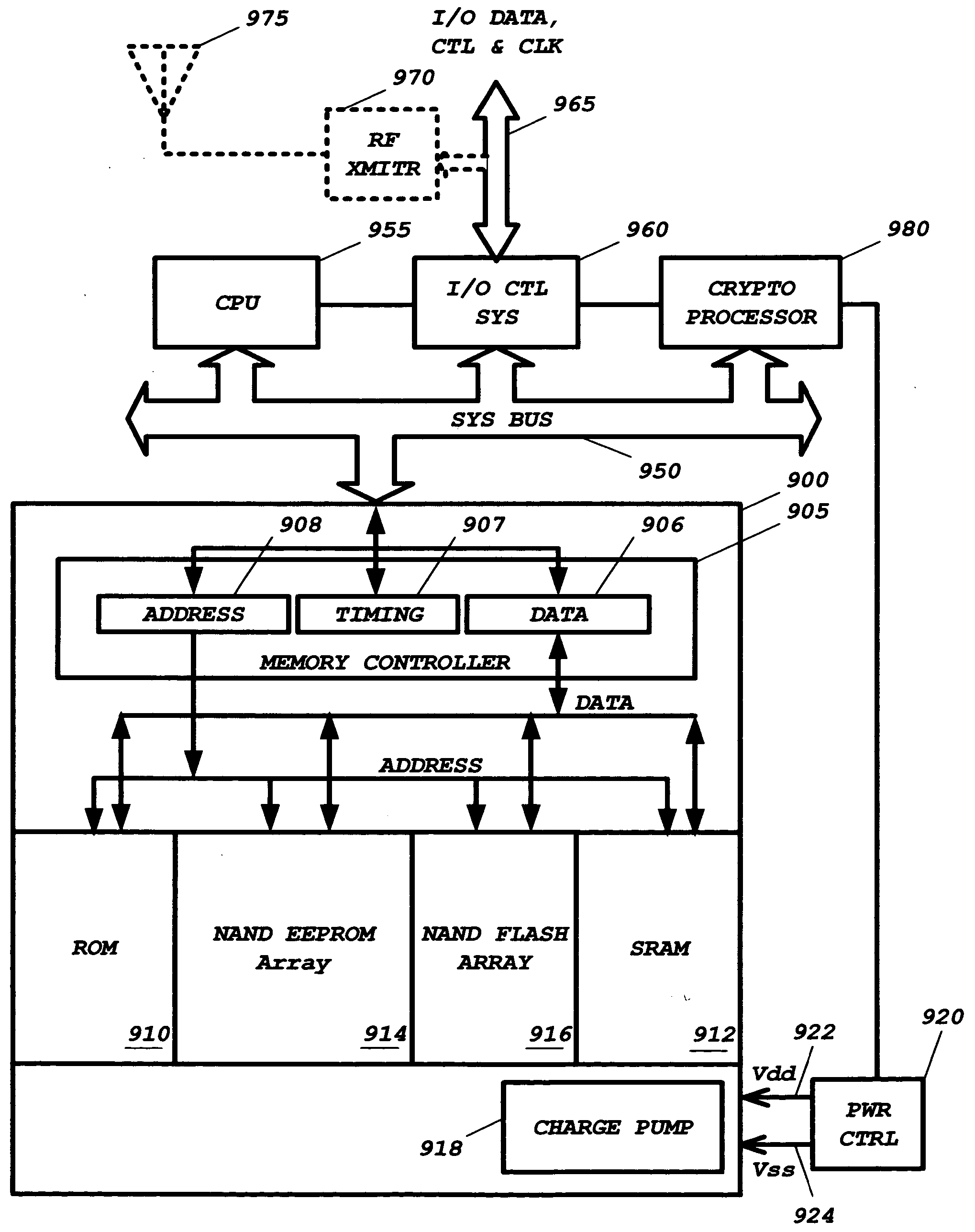
[0062] A combination volatile and nonvolatile memory integrated circuit of this invention incorporates at least one volatile memory array (SRAM, PSRAM, or DRAM), at least one mask programmable ROM, and multiple NAND configured nonvolatile memory arrays within the same integrated circuit. A memory control circuit is connected to communicate with external circuitry to receive address, command, and data signals, to interpret said address, command, and data signals. The memory control circuit develops the necessary timing and control signals to transfer the address, command and data signals for reading, writing, programming, and erasing the volatile and nonvolatile memory arrays.

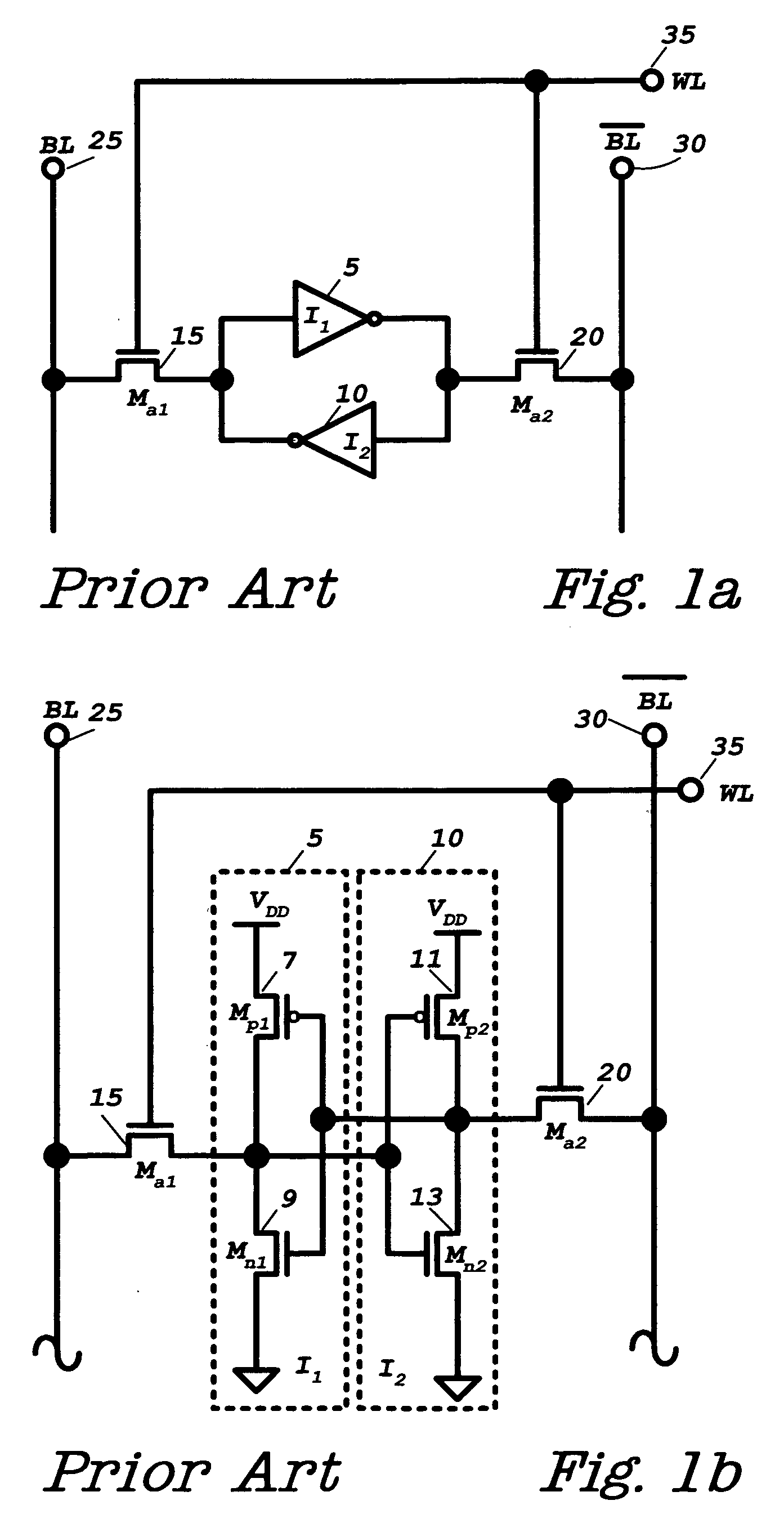
[0063] The SRAM as incorporated in the combination volatile and nonvolatile memory integrated circuit of this invention is as described above for FIGS. 1a and 1b.

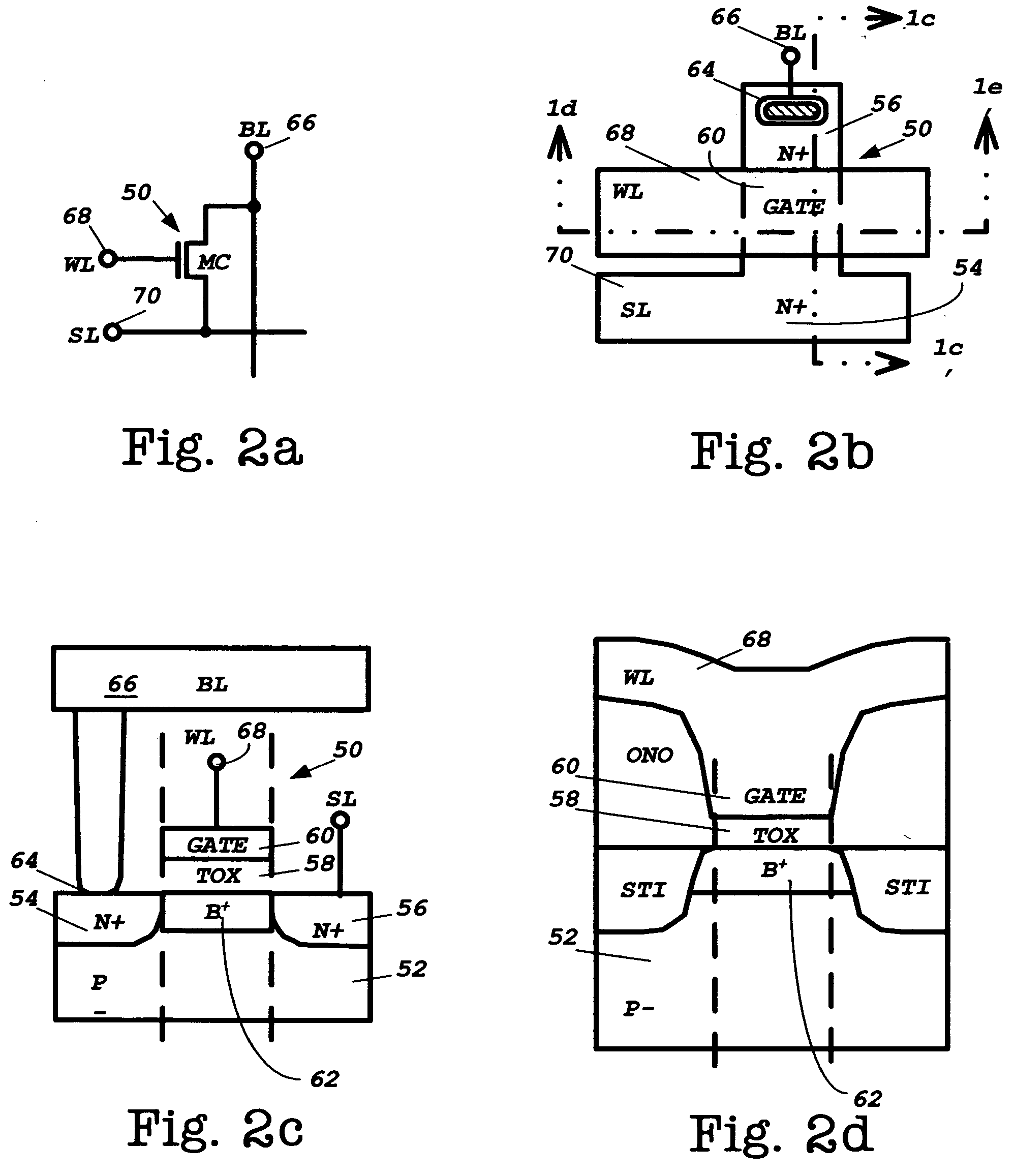
[0064] A mask programmable ROM memory cell as incorporated in the combination volatile and nonvolatile memory integrated circuit of this invention is...


PUM


Abstract

A combination volatile and nonvolatile memory integrated circuit has at least one volatile memory array placed on the substrate and multiple nonvolatile memory arrays. The volatile and nonvolatile memory arrays have address space associated with each other such that each array may be addressed with common addressing signals. The combination volatile and nonvolatile memory integrated circuit further has a memory control circuit in communication with external circuitry to receive address, command, and data signals. The memory control circuit interprets the address, command, and data signals, and for transfer to the volatile memory array and the nonvolatile memory arrays for reading, writing, programming, and erasing the volatile and nonvolatile memory arrays. The volatile memory array is may be a SRAM, a pseudo SRAM, or a DRAM. Any of the nonvolatile memory arrays maybe masked programmed ROM arrays, NAND configured flash memory NAND configured EEPROM.

Description

RELATED PATENT APPLICATIONS [0001] This application claims priority to U.S. Provisional Patent Application Ser. No. 60 / 640,080, filed on Dec. 28, 2004, which is herein incorporated by reference. [0002]“A Novel Monolithic, Combination Nonvolatile Memory Allowing Byte, Page a Cell Array Using a Unified Cell Structure and Technology with a New Scheme of Decoder and Layout ”, U.S. patent application Ser. No. 10 / 223,208, filed Aug. 19, 2002, assigned to the same assignee as the present invention, and herein incorporated by reference. [0003]“A Novel Monolithic, Combination Nonvolatile Memory Allowing Byte, Page and Block Write with No Disturb and Divided-Well in the Cell Array Using a Unified Cell Structure and Technology with a New Scheme of Decoder and Layout”, U.S. patent application Ser. No. 10 / 351,180, filed Jan. 24, 2003, assigned to the same assignee as the present invention, and herein incorporated by reference. [0004]“A Combination Nonvolatile Memory Using Unified technology with...

Claims


Application Information

Patent Timeline
IPC IPC(8): G06K19/06
CPCG11C11/005G11C16/0408G11C16/0483G11C17/12H01L27/115H01L29/0646H01L29/7885H10B69/00
Inventor LEE, PETER W.
Owner CALLAHAN CELLULAR L L C
Why Eureka
Try Eureka