Semiconductor device and method of forming same

a semiconductor device and semiconductor technology, applied in the direction of semiconductor devices, electrical equipment, transistors, etc., can solve the problems of severe short channel effect, leakage current of semiconductor devices may increase, and malfunction of semiconductor devices may aris

Inactive Publication Date: 2006-06-29
SAMSUNG ELECTRONICS CO LTD
View PDF6 Cites 22 Cited by
  • Summary
  • Abstract
  • Description
  • Claims
  • Application Information

AI Technical Summary

Problems solved by technology

Accordingly, channel length of a MOS transistor is gradually reduced to result in severe short channel effects.
Since turn-off current of the MOS transistor increases due to the threshold voltage roll-off, leakage current of a semiconductor device may increase or malfunction of a semiconductor device may arise.
Unfortunately, this approach may make the short channel effects severe.

Method used


Image

  • Semiconductor device and method of forming same
  • Semiconductor device and method of forming same
  • Semiconductor device and method of forming same

Examples


first embodiment

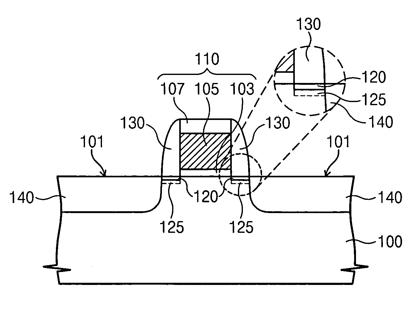
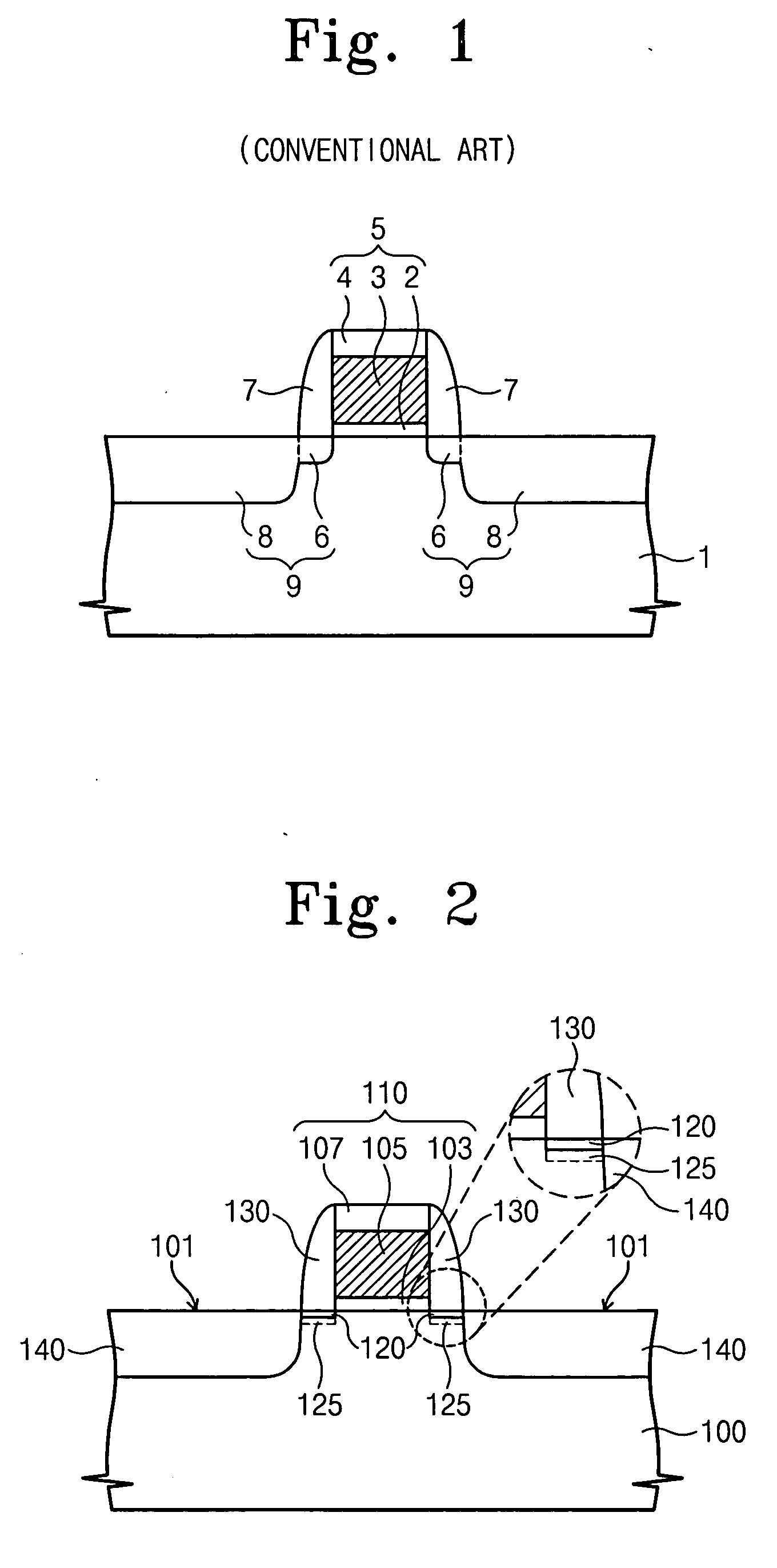
[0026]FIG. 2 is a cross-sectional view of a semiconductor device according to the present invention. Referring to FIG. 2, a gate pattern 110 is disposed on a semiconductor substrate 100 doped with impurities of a first conduction type. The gate pattern 110 may include a gate insulation layer 103, a gate electrode 105, and a capping pattern 107, which are stacked in the order named. The gate insulation layer 103 may be made of thermal oxide. The gate electrode 105 may be made of material selected from the group consisting of doped polysilicon, metal (e.g., tungsten or molybdenum), conductive metal nitride (e.g., titanium nitride or tantalum nitride), metal silicide (e.g., tungsten silicide, cobalt silicide, nickel silicide or titanium nitride), and combinations thereof. The capping pattern 107 may be an insulation pattern made of material selected from the group consisting of silicon oxide, silicon oxynitride, and silicon nitride.

[0027] A gate spacer 130 is disposed on both sidewalls...

second embodiment

[0070]FIG. 9 is a cross-sectional view of a semiconductor device according to the present invention. Referring to FIG. 9, a gate pattern 210 is disposed on a semiconductor substrate 200 doped with impurities of a first conduction type. The gate pattern 210 includes a gate insulation layer 203, a gate electrode 205, and a capping pattern 207, which are stacked in the order named. A gate spacer 230 is disposed on both sidewalls of the gate pattern 210.

[0071] A fixed charge layer 220 is disposed in the semiconductor substrate 200 below the gate spacer 230. The fixed charge layer 220 is disposed directly below a substrate surface 201. The fixed charge layer 220 generates positive or negative fixed charges. Therefore, the fixed charge layer 220 is charged with positive or negative charges. Elements in the fixed charge layer are segregated to the substrate surface 201 to the inside of the semiconductor substrate 200 by heat.

[0072] A lightly doped layer 215 overlapping the fixed charge la...


PUM


Abstract

A semiconductor device includes a gate pattern disposed on a semiconductor substrate, a gate spacer disposed on both sidewalls of the gate pattern, and a fixed charge layer disposed in the semiconductor substrate below the gate spacer. Elements generating fixed charges are injected into the fixed charge layer. A layer in which carriers induced by the fixed charge layer are accumulated is disposed below the fixed charge layer. The elements are segregated to a substrate of the semiconductor substrate from the inside of the semiconductor substrate by heat.

Description

RELATED APPLICATION [0001] This application claims priority from Korean Patent Application No. 2004-115406, filed on Dec. 29, 2004 in the Korean Intellectual Property Office, the disclosure of which is incorporated herein in its entirety by reference. FIELD OF THE INVENTION [0002] The present invention relates generally to semiconductor devices and, more particularly, to semiconductor devices having source / drain regions and methods of forming the same. BACKGROUND OF THE INVENTION [0003] A MOS transistor of a semiconductor device may include a pair of source / drain regions disposed at a semiconductor substrate and spaced apart from each other and a gate electrode disposed over a channel region between the pair of the source / drain regions. A typical MOS transistor includes a source / drain region of a lightly doped drain (LDD) structure to reduce hot carrier effects. A lightly doped region is formed at a portion of a source / drain region adjacent to a channel region, so that concentration...

Claims


Application Information

Patent Timeline
Patent Type & Authority Applications(United States)
IPC IPC(8): H01L29/76H01L29/788H01L29/94
CPCH01L21/26506H01L21/28273H01L21/28282H01L29/6659H01L29/66825H01L29/66833H01L29/78H01L29/7833H01L29/7881H01L29/40114H01L29/40117H01L21/18
Inventor BUH, GYOUNG-HOSHIN, YU-GYUNRYOO, CHANG-WOOHONG, SOO-JINLEE, JIN-WOOKYON, GUK-HYON
Owner SAMSUNG ELECTRONICS CO LTD
Why Eureka
Try Eureka