Semiconductor device and method of manufacturing the same

a technology of semiconductors and semiconductors, applied in the direction of semiconductor devices, electrical devices, transistors, etc., can solve the problems of local current crowding at the depletion layer, difficulty in fine patterning of the size, and serge voltag

Inactive Publication Date: 2006-06-29
KK TOSHIBA
View PDF13 Cites 27 Cited by
  • Summary
  • Abstract
  • Description
  • Claims
  • Application Information

AI Technical Summary

Problems solved by technology

The device with such the structure causes a problem, however, because a large number of process steps are required for production and fine patterning of the size is difficult in the lateral direction or along the channel length.
The semiconductor device with the triple-layered pillar structure, however, causes a serge voltage when the power MOSFET transits the state from conductive to non-conductive.
If a serge voltage arises in such the condition, it causes local current crowding at the depletion layer.
When the extent of the current crowding exceeds an acceptable value (avalanche withstand capability), it leads to device destruction at a high possibility.

Method used


Image

  • Semiconductor device and method of manufacturing the same
  • Semiconductor device and method of manufacturing the same
  • Semiconductor device and method of manufacturing the same

Examples


first embodiment

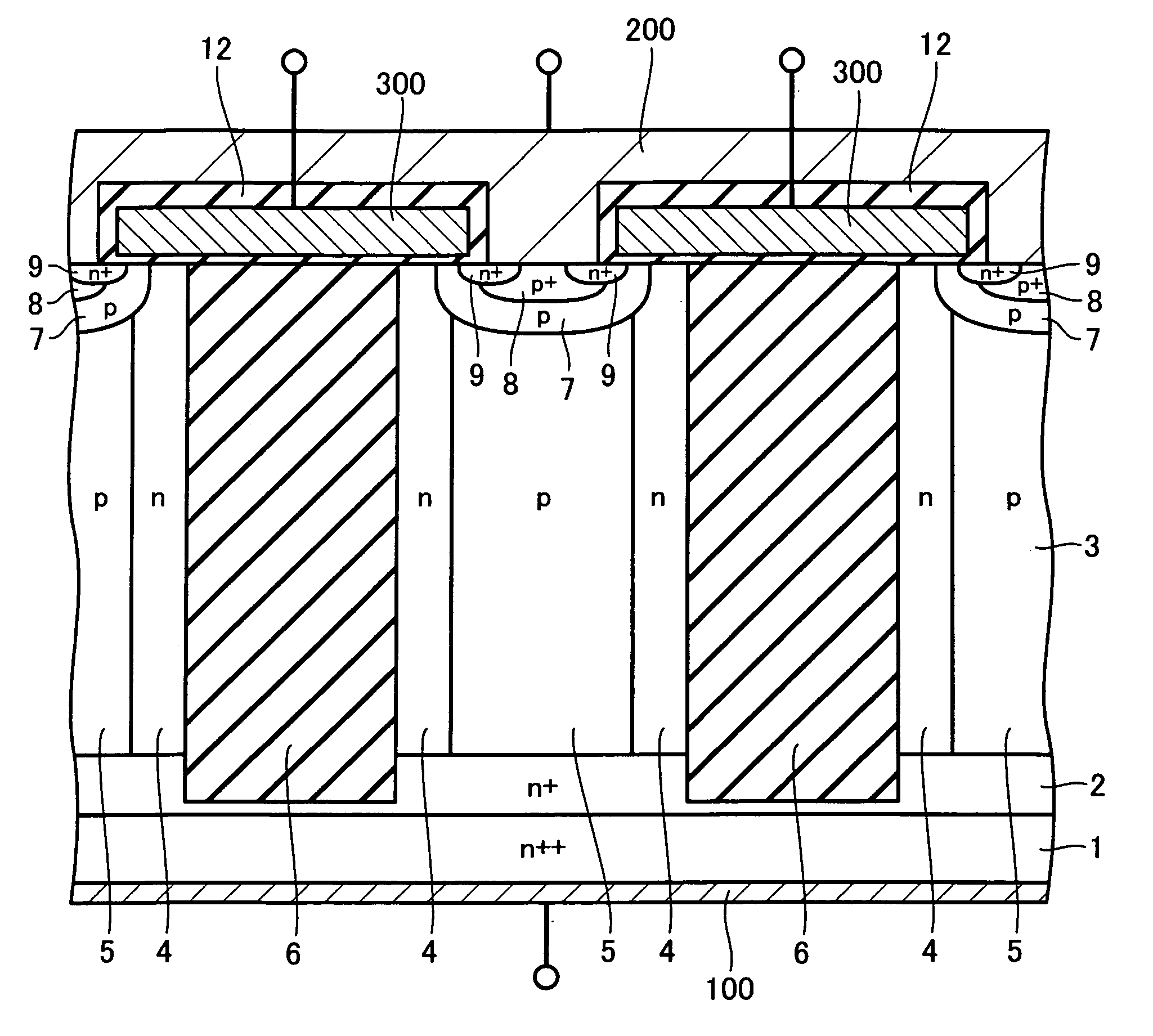
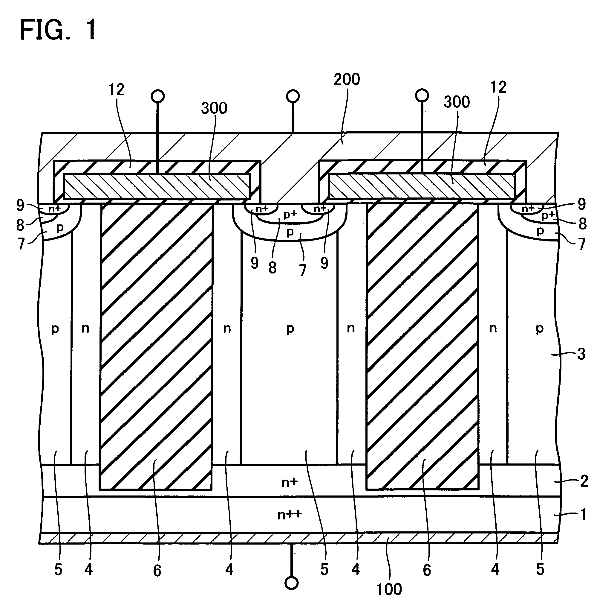
[0034]FIG. 1 shows part of a sectional structure of a deep trench MOSFET (DTMOSFET) according to the present invention.

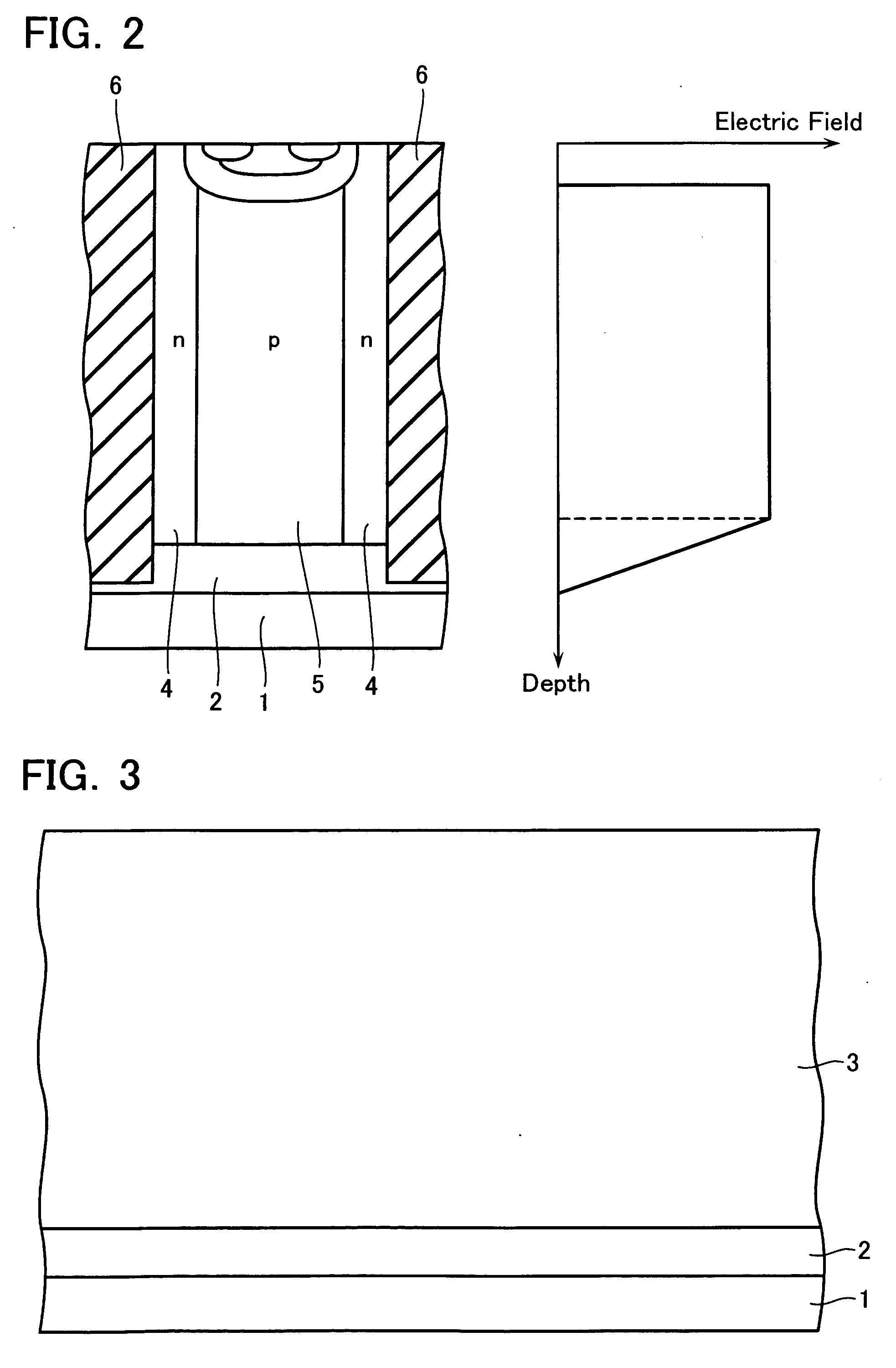
[0035] The DTMOSFET comprises an n++-type semiconductor substrate 1, which serves as a common drain of MOSFETs that are isolated from each other with a device isolation film 6. The semiconductor substrate 1 is connected to a drain electrode 100. An n+-type middle layer 2 is formed over the semiconductor substrate 1. A pillar layer 3 is formed on the middle layer 2 between portions of the device isolation film 6. The pillar layer 3 includes an n-type pillar layer 4 and a p-type pillar layer 5, which are formed into strips in the vertical direction and arranged alternately.

[0036] The middle layer 2 has an impurity concentration lower than that of the semiconductor substrate 1 and higher than that of the n-type pillar layer 4 by 2.5-30 times. For example, the impurity concentration in the middle layer 2 is determined approximately from 5.0E15 to 6.0E16 (cm sub −3) whe...


PUM


Abstract

A semiconductor substrate of a first conduction type is provided for serving as a common drain to a plurality of power MISFET cells. A middle semiconductor layer is formed on the semiconductor substrate and has a lower impurity concentration than that of the semiconductor substrate. Pillar regions are formed on the middle semiconductor layer and include semiconductor regions of the first conduction type having a lower impurity concentration than that of the middle semiconductor layer.

Description

CROSS-REFERENCE TO RELATED APPLICATION [0001] This application is based upon and claims the benefit of priority from the prior Japanese Patent Application No. 2004-379009, filed on Dec. 28, 2004, the entire content of which is incorporated herein by reference. BACKGROUND OF THE INVENTION [0002] 1. Field of the Invention [0003] The present invention relates to a semiconductor device including a plurality of vertical power MISFET cells and method of manufacturing the same. [0004] 2. Description of the Related Art [0005] Development of a semiconductor device has been proceeded to achieve both a higher breakdown voltage and a lower on-resistance in a power MOSFET at the same time. [0006] For example, a semiconductor device called Super Junction structure has been proposed by Deboy, G., et al. in “A New Generation of High Voltage MOSFETs Breaks the Limit of Silicon”, IEDM Tech. Dig. (1998), P683-686. The device with such the structure causes a problem, however, because a large number of ...

Claims


Application Information

Patent Timeline
Patent Type & Authority Applications(United States)
IPC IPC(8): H01L29/76
CPCH01L21/26586H01L29/0634H01L29/0653H01L29/0878H01L29/66712H01L29/7802H01L29/7811
Inventor KOUZUKI, SHIGEOOKUMURA, HIDEKISAITO, WATARUIZUMISAWA, MASARUSHIOMI, MASAHIKOKOBAYASHI, HITOSHITOKANO, KENICHIYANAGISAWA, SATOSHIYOSHIOKA, HIRONORIKIMURA, MANABU
Owner KK TOSHIBA
Why Eureka
Try Eureka