Solid-state imaging device and method for making the same

Inactive Publication Date: 2006-07-06
SONY CORP
View PDF3 Cites 9 Cited by
  • Summary
  • Abstract
  • Description
  • Claims
  • Application Information

AI Technical Summary

Benefits of technology

[0019] According to still another embodiment of the present invention, there is provided a method for making a solid-state imaging device, the method including an interlayer insulating film forming step for forming an interlayer insulating film on or above a semiconductor substrate so that generation of capacitance between the semiconductor substrate and a metal wire to be formed is prevented; a diffusion preventing film forming step of forming a diffusion preventing film for preventing diffusion of the metal wire, the diffusion preven

Problems solved by technology

According to the solid-state imaging device disclosed in Japanese Unexamined Patent Application Publication No. 2003-324189, a step of selectively removing the Cu-diffusion preventing film overlaying the sensor and the step of burying the new film in the removed region are needed after the deposition of the Cu-diffusion preventing film on the wirin

Method used


Image

  • Solid-state imaging device and method for making the same
  • Solid-state imaging device and method for making the same
  • Solid-state imaging device and method for making the same

Examples


Example

First Embodiment

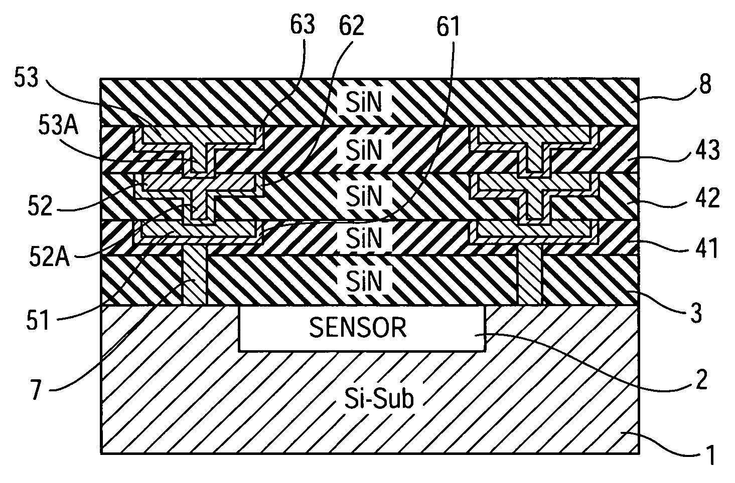
[0025] A solid-state imaging device and a production method therefor will now be described with reference to drawings.

[0026]FIG. 1 is a cross-sectional view of a solid-state imaging device and a production method therefor according to a first embodiment.

[0027] As shown in FIG. 1, the solid-state imaging device of the first embodiment includes a silicon (Si) substrate 1 including a sensor 2, which is a photoelectric transducer such as a photodiode; and metal wires 51, 52, and 53 stacked on the Si substrate 1. An interlayer insulating film 3 for preventing generation of capacitance between the Si substrate 1 and the metal wires 51, 52, and 53 is disposed on the Si substrate 1, and wiring interlayer films 41, 42, and 43 are sequentially formed on the interlayer insulating film 3. A protective film 8 is disposed on the wiring interlayer film 43.

[0028] A color filter and an on-chip lens are disposed on the protective film 8 but are not shown in the drawings since they...

Example

Second Embodiment

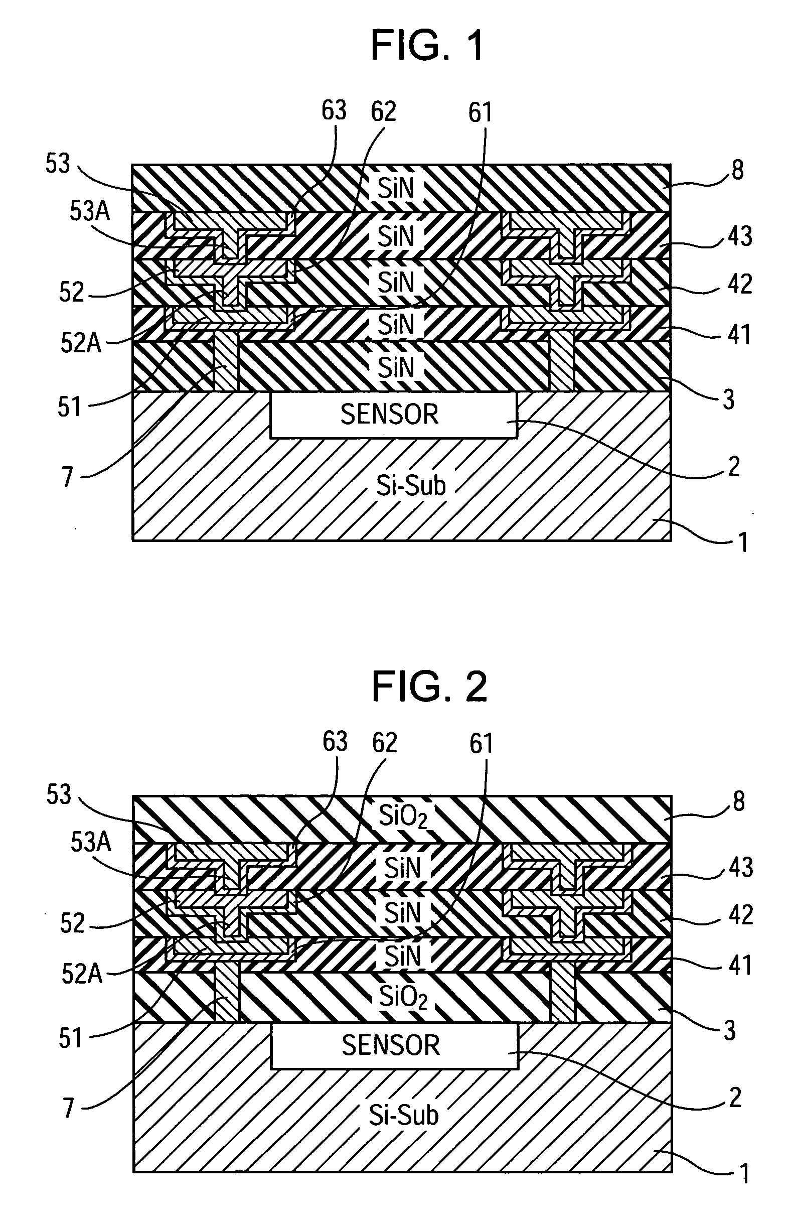
[0035]FIG. 2 is a cross-sectional view showing a solid-state imaging device and a production method therefor according to a second embodiment.

[0036] As shown in FIG. 2, the solid-state imaging device and the method of the second embodiment are different from those of the first embodiment shown in FIG. 1 in that, while the wiring interlayer films 41, 42, and 43 are composed of the same diffusion preventing material such as silicon nitride or silicon carbide, the interlayer insulating film 3 and the protective film 8 are composed of a material different from the diffusion preventing material. For example, the interlayer insulating film 3 and the protective film 8 are composed of silicon oxide.

[0037] According to the structure of the second embodiment, although diffusion of the metal wire 53 occurs from the top surface, the diffusion into the wiring interlayer film 43 is prevented.

[0038] Moreover, there are only two interfaces between the layers having different re...

Example

Third Embodiment

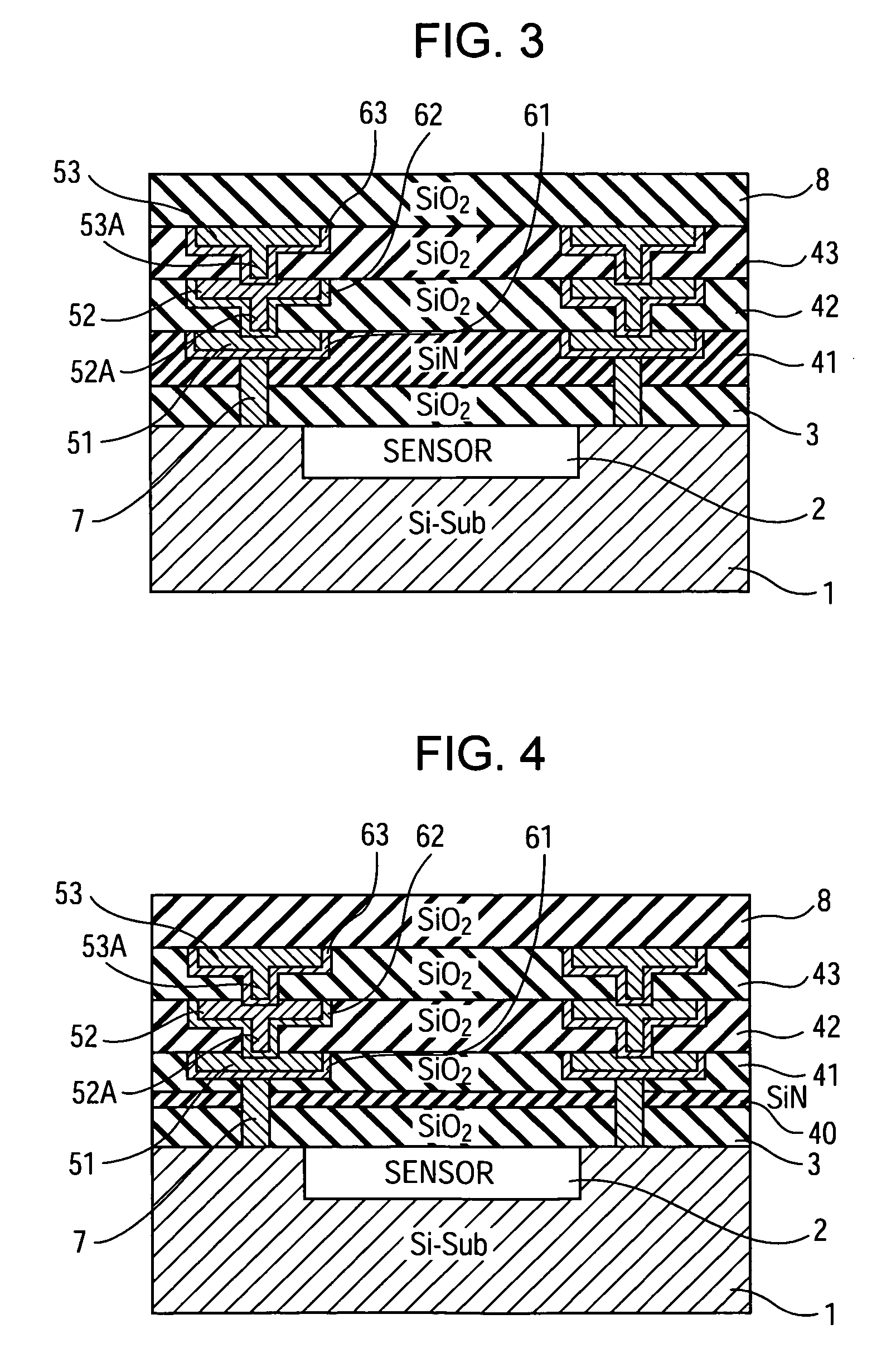
[0039]FIG. 3 is a cross-sectional view showing a solid-state imaging device and a production method therefor according to a third embodiment.

[0040] As shown in FIG. 3, the solid-state imaging device and the method of the third embodiment differ from those of the first embodiment shown in FIG. 1 in that the lowermost wiring interlayer film, i.e., the wiring interlayer film 41, among the wiring interlayer films 41, 42, and 43 is composed of the same diffusion preventing material (silicon nitride or silicon carbide) as that used in the first embodiment, and that the wiring interlayer films 42 and 43, the interlayer insulating film 3, and the interlayer insulating film 3 are composed of a material, e.g., silicon oxide, different from the diffusion preventing material.

[0041] According to the third embodiment, although the metal wires 51, 52, and 53 diffuse from upper surfaces, diffusion into the wiring interlayer film 41 is prevented.

[0042] Moreover, there are only tw...


PUM


Abstract

A solid-state imaging device includes a semiconductor substrate, one or more wiring interlayer films disposed on or above the semiconductor substrate, and one or more metal wires embedded in the wiring interlayer films. The one or more wiring interlayer films are composed of a diffusion preventing material that prevents the diffusion of the metal wire.

Description

CROSS REFERENCES TO RELATED APPLICATIONS [0001] The present invention contains subject matter related to Japanese Patent Application JP 2004-357602 filed in the Japanese Patent Office on Dec. 10, 2004, the entire contents of which are incorporated herein by reference. BACKGROUND OF THE INVENTION [0002] 1. Field of the Invention [0003] The present invention relates to a solid-state imaging device having a diffusion preventing film for preventing diffusion of metal constituting wires formed on or above a semiconductor substrate in which a plurality of photoelectric transducers are formed. The present invention also relates to a method for making the solid-state imaging device. [0004] 2. Description of the Related Art [0005] In recent years, as the semiconductor integrated circuits become finer, copper (Cu) wires are increasingly used, which activates the development of Cu-wiring processes. Formation of Cu wires is carried out by a damascene process with high production efficiency. [00...

Claims


Application Information

Patent Timeline
IPC IPC(8): H01L23/52H01L21/768H01L23/522H01L27/14H04N5/335H04N5/369
CPCH01L27/14636H01L27/14683
Inventor TAKEDA, TAKESHI
Owner SONY CORP
Why Eureka
Try Eureka