

Image sensor and method of fabricating the same
a technology of image sensor and manufacturing method, applied in the field of image sensor, can solve problems such as failure of function, and achieve the effect of improving concentration efficiency and preventing eroded
- Summary
- Abstract
- Description
- Claims
- Application Information
AI Technical Summary
Benefits of technology
Problems solved by technology
Method used
Image

Examples
first embodiment
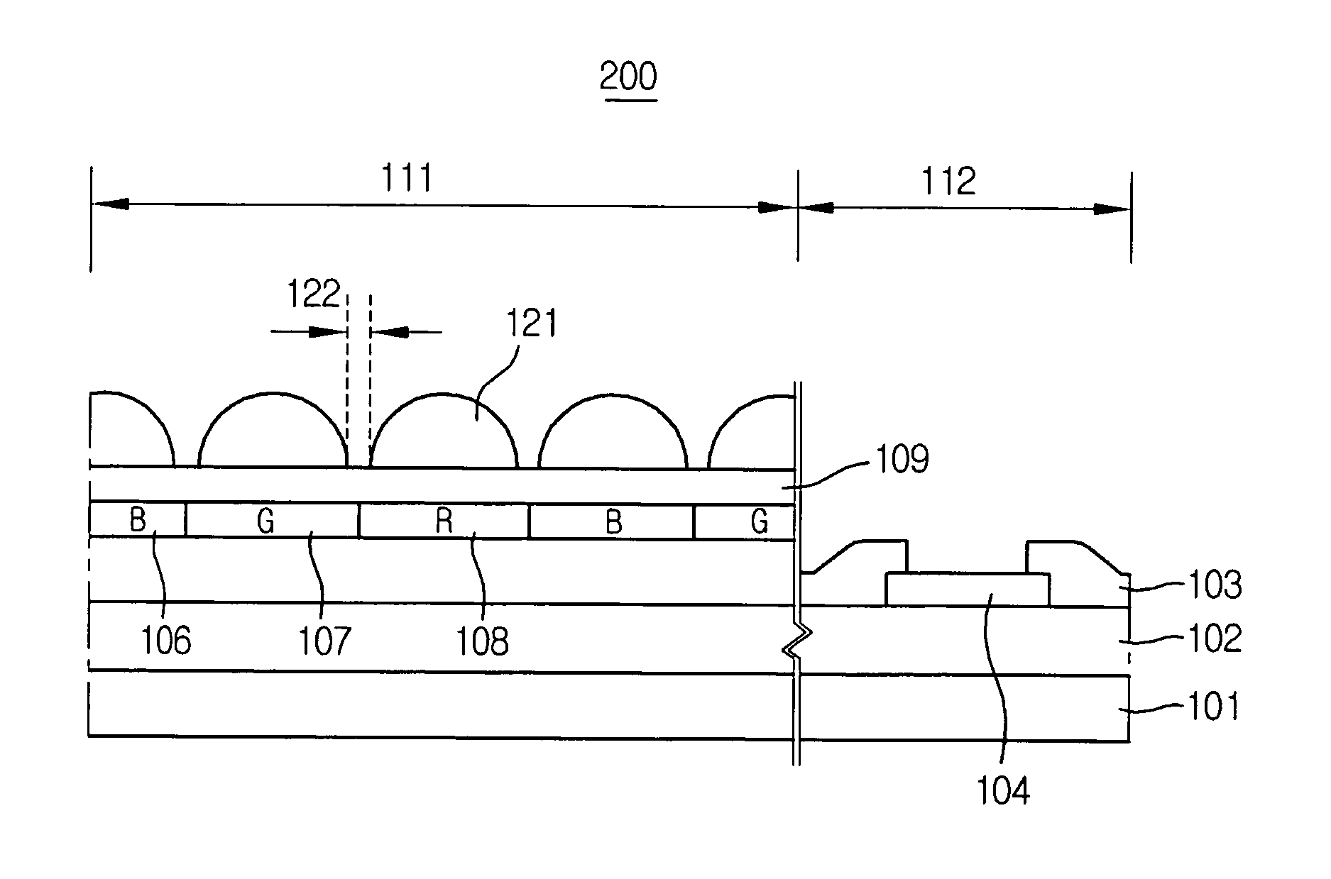
[0028]FIG. 2 is a schematic sectional view of an image sensor 200 to which a method of fabricating the image sensor according to the present invention is applied, and omits a photodiode and the like.
[0029] The image sensor 200 according to a first embodiment of the present invention is characterized in that the image sensor 200 includes an overcoating layer 109 and at least two micro lenses 121, and the overcoating layer 109 positioned below a clearance between the micro lenses 121 is etched and curved surfaces of the micro lenses 121 extend.
[0030] At this time, the image sensor 200 is characterized by including a substrate 101 divided into a pixel array area 111 and a bonding pad area 112, an element layer 102 formed on the substrate 101, a bonding pad 104 formed on a bonding pad area of the element layer 102, a passivation layer 103 covering the bonding pad 104 and formed on the element layer 102, color filter layer including a plurality of color filter patterns 106, 107, 108 seq...
second embodiment
[0042]FIG. 6 is a schematic sectional view of an image sensor 300 according to the present invention, and omits a photodiode and the like.
[0043] The image sensor 300 according to a second embodiment of the present invention is characterized in that the image sensor 300 includes an overcoating layer 109 and at least two micro lenses 121, and the overcoating layer 109 positioned below a clearance between the micro lenses 121 is etched and curved surfaces of the micro lenses 121 extend.
[0044] The image sensor 300 according to the second embodiment of the present invention is different from that according to the first embodiment in that while the partially remaining passivation layer 103 is etched, the overcoating layer 109 positioned below the clearance between the micro lenses 121 is etched such that the surfaces of the micro lenses 121 extend.
[0045] A method of fabricating the image sensor 300 according to the second embodiment of the present invention will now be described with re...
third embodiment
[0053]FIG. 7 is a schematic sectional view of an image sensor 400 according to the present invention, and omits a photodiode and the like.
[0054] The image sensor 400 according to the third embodiment of the present invention is characterized by including at least two micro lenses 121 and a non-fluid film 125 filling a clearance between the adjacent micro lenses 121 and formed on the at least two micro lenses 121.
[0055] Comparing the image sensor 400 according to the third embodiment with the image sensor 200 according to the first embodiment, the image sensor 400 is different from the image sensor 200 in that the image sensor 400 includes the non-fluid film 125 which fills the clearance between the adjacent micro lenses 121, has a greater refractivity than the micro lenses 121 and is formed on the micro lenses 121.
[0056] The fabrication method of the image sensor 400 according to the third embodiment is the same as that according to the first embodiment until the micro lenses 121 ...
PUM
| Property | Measurement | Unit |
|---|---|---|
| area | aaaaa | aaaaa |
| time | aaaaa | aaaaa |
| thick | aaaaa | aaaaa |
Abstract
Description
Claims
Application Information