Semiconductor apparatus and manufacturing method

a technology of semiconductor devices and manufacturing methods, applied in the direction of rotary stirring mixers, separation processes, transportation and packaging, etc., can solve the problems of poor wettability of lead frame materials ni or cu, chip cracking, and inability to perform excellent die bonding, so as to prevent chip cracking in die bonding

Inactive Publication Date: 2006-07-13
RENESAS ELECTRONICS CORP
View PDF4 Cites 27 Cited by
  • Summary
  • Abstract
  • Description
  • Claims
  • Application Information

AI Technical Summary

Benefits of technology

[0013] Effect obtained by the exemplars of the invention disclosed herein will be described briefly below.
[

Problems solved by technology

Thus, there arises a problem that the chip may be cracked.
In addition, the wettability with a lead frame material of Ni or Cu is low due to Al forming a solid oxide film on the solder material.
Thus, there is a problem that excellent die bonding cannot be performed.
Thus, there is a problem that the chip exfoliates by cracking at the solder joint layer.
Further, in a temperature cycle test where a temperature change caused by heating of the semiconductor device is simulated, there is a

Method used


Image

  • Semiconductor apparatus and manufacturing method
  • Semiconductor apparatus and manufacturing method
  • Semiconductor apparatus and manufacturing method

Examples


embodiments

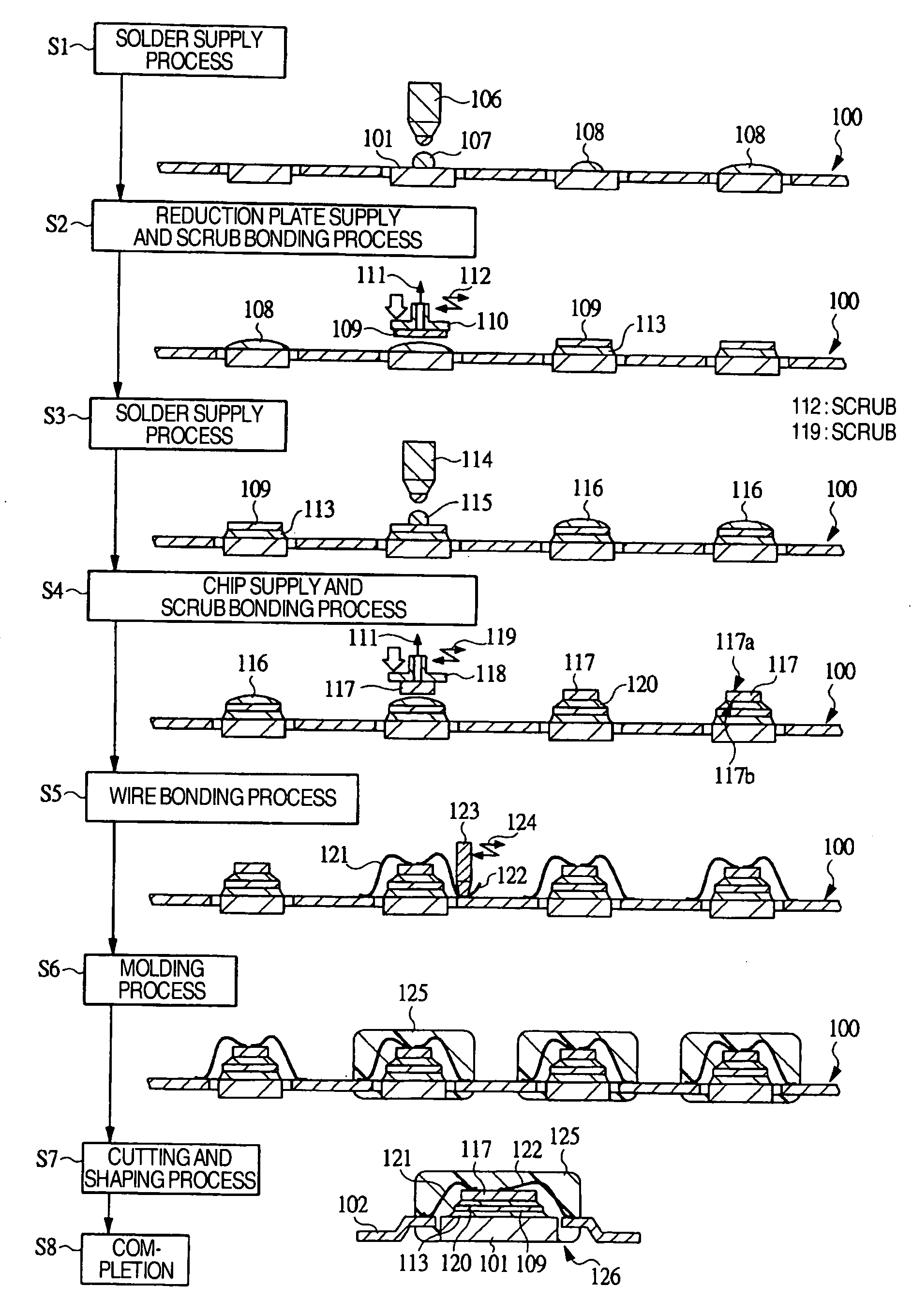
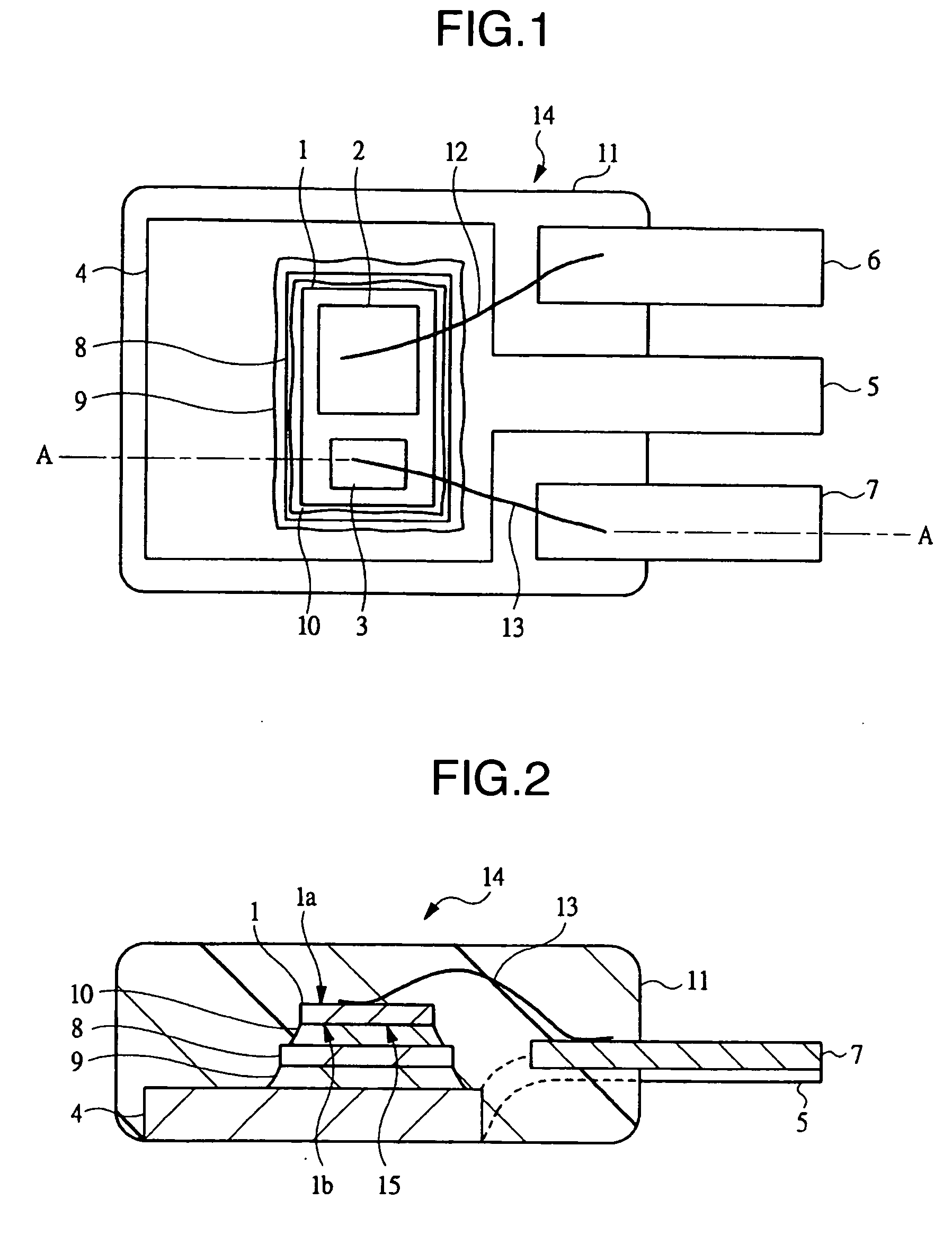
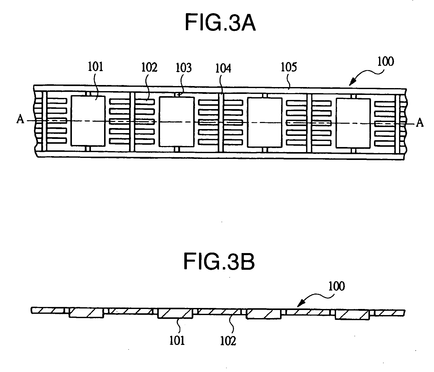
[0040]FIG. 1 is a plan view showing an example of an internal structure of a semiconductor apparatus according to an embodiment of the present invention with an encapsulant regarded as transparent; FIG. 2 is a sectional view showing the section taken on line A-A in FIG. 1; FIG. 3A is a partial plan view showing an example of the structure of a lead frame used for assembling the semiconductor apparatus according to the embodiment of the present invention; FIG. 3B is a partial sectional view showing a section of the same taken on line A-A in FIG. 3A; FIG. 4 is a manufacturing process flow chart showing an example of an assembling procedure of the semiconductor apparatus according to the embodiment of the present invention; FIG. 5 is a result data table showing an example of evaluation results of the semiconductor apparatus according to the embodiment of the present invention, in which a thermal stress reduction plate and solder incorporated in the semiconductor apparatus were set as p...


PUM

PropertyMeasurementUnit
Temperatureaaaaaaaaaa
Fractionaaaaaaaaaa

Abstract

Pb free solder is used in die bonding. A thermal stress reduction plate is disposed between a semiconductor chip and a die pad made of a Cu alloy. The semiconductor chip and the thermal stress reduction plate are joined and the thermal stress reduction plate and the die pad are joined by a joint material of Pb free solder having Sn—Sb—Ag—Cu as its main constituent elements and having a solidus temperature not lower than 270° C. and a liquidus temperature not higher than 400° C. Thus, die bonding can be performed using the Pb free solder without generating any chip crack.

Description

BACKGROUND OF THE INVENTION [0001] The present invention relates to a semiconductor apparatus and a technique for manufacturing the same, and particularly relates to a technique effective in application to Pb free solder for fixing a semiconductor device. [0002] A background-art alloy member for die bonding uses a pure Al plate or a 42 alloy material 0.05-0.5 mm thick as a substrate, and an alloy joint layer 0.005-0.1 mm thick is provided on each surface of the substrate. [0003] Further, a Pb free alloy having a liquidus temperature not higher than 400° C. and a solidus temperature not lower than 280° C. or a Pb free alloy having a liquid-phase volume ratio not higher than 15% at 280° C. is used as the alloy joint layer (e.g. JP-A-2001-127076 (pp. 2-3)). [0004] The following four items are important to properties of a solder material applicable to die bonding for a semiconductor apparatus. The first item is a condition as to a process temperature. To make it possible to perform die ...

Claims


Application Information

Patent Timeline
IPC IPC(8): H01L21/50H01L23/28H01L21/48
CPCH01L2224/29111H01L2924/01029H01L2924/01047H01L2924/01051H01L2924/0103H01L2924/01079H01L23/3107H01L23/3677H01L23/3735H01L23/4334H01L23/49537H01L23/49562H01L23/49575H01L24/06H01L24/27H01L24/29H01L24/32H01L24/33H01L24/45H01L24/743H01L24/78H01L24/83H01L24/85H01L24/97H01L2224/04042H01L2224/05553H01L2224/05624H01L2224/05647H01L2224/0603H01L2224/291H01L2224/45124H01L2224/48091H01L2224/48247H01L2224/48472H01L2224/49171H01L2224/73265H01L2224/743H01L2224/78H01L2224/83192H01L2224/83801H01L2224/85181H01L2224/85205H01L2224/92H01L2224/92247H01L2224/97H01L2924/01004H01L2924/01005H01L2924/01013H01L2924/01014H01L2924/01015H01L2924/01022H01L2924/01027H01L2924/01028H01L2924/01033H01L2924/0105H01L2924/01073H01L2924/01075H01L2924/01078H01L2924/01082H01L2924/014H01L2924/19043H01L2924/00014H01L2224/85H01L2224/83H01L2924/01039H01L2224/32245H01L2924/12041H01L24/48H01L24/49H01L2224/29H01L2224/29298H01L2924/01006H01L2924/01019H01L2924/01023H01L2924/01024H01L2224/29101H01L2924/00H01L2924/0132H01L2924/0133H01L2924/0134H01L2924/00013H01L2224/29299H01L2224/2929H01L2224/48724H01L2224/48747H01L2924/3512H01L2224/29099H01L2224/29199H01L2924/01032H01L2924/00012H01L2924/01031H01L2924/01012H01L2924/01026H01L2924/01083H01L2924/10253H01L2924/351H01L2224/29294H01L2924/181H01L2224/83206H01L2224/78301H01L24/73H01L2224/83385H01L2224/75611H01L2224/2612B01D21/286C02F1/5209B01F27/906
Inventor KAJIWARA, RYOUICHIITOU, KAZUTOSHIKAGII, HIDEMASAOKA, HIROINAKAMURA, HIROYUKI
Owner RENESAS ELECTRONICS CORP
Why Eureka
Try Eureka