Semiconductor package with heat sink

a technology of heat sink and semiconductor, applied in the direction of semiconductor devices, semiconductor/solid-state device details, electrical apparatus, etc., can solve the problems of dislocation of heat sink, difficult to firmly adhere and position heat sink on substrate, severe situation, etc., to increase the contact area, enhance the anchoring effect, and increase the contact area

Active Publication Date: 2005-02-15
SILICONWARE PRECISION IND CO LTD
View PDF16 Cites 22 Cited by
  • Summary
  • Abstract
  • Description
  • Claims
  • Application Information

AI Technical Summary

Benefits of technology

The above semiconductor packages according to the invention yield significant benefits in the use of a heat sink formed with at least one burr at a position where an adhesive material for attaching the heat sink to a substrate can submerge the burr. In particular, the heat sink is composed of a flat portion and a support portion, wherein the flat portion is elevated above a chip mounted on the substrate, and the support portion is attached to the substrate by the adhesive material. The burr is located on an inner surface of the support portion that faces toward the chip, and can be submerged by the adhesive material, thereby increasing the contact area between the heat sink and the adhesive material, and making the adhesive material provide an anchoring effect to firmly secure the heat sink to the substrate. Besides, the support portion of the heat sink can be formed with a recess portion at a position in contact with the substrate, and at least one burr is located on an interior surface of the recess portion. The recess portion can be a groove or blind cavity. The adhesive material applied between the support portion and the heat sink can fill the recess portion and submerge the burr. The provision of the recess portion and the burr further increases the contact area between the heat sink and the adhesive material, thereby enhancing the anchoring effect from the adhesive material to allow the heat sink to be strongly held on the substrate in position. Therefore, there is no need to form prior-art holes on the substrate for accommodating fixing members such as bolts used to connect the heat sink and the substrate, such that circuit layout and solder ball arrangement on the substrate would not be adversely affected, and thus the substrate can be desirably implanted with a full array of solder balls. Moreover, the substrate free of holes prevents the entrance of external moisture or contaminant and thereby eliminates reliability issues. In addition, the heat sink is mounted on the substrate instead of on the chip, thereby preventing chip cracks that occur in the prior art with the heat sink directly stacked on the chip.

Problems solved by technology

However, the provision of passive component undesirably decreases area on the substrate available for contact with the heat sink, making the heat sink relatively difficult to be firmly adhered and positioned onto the substrate and thereby leading to dislocation of the heat sink.
This situation becomes severe in the use of a large heat sink.
Moreover, attachment between the heat sink and the substrate via the adhesive or solder would be damaged by unsatisfactory cleanness of contact surfaces between the heat sink and the substrate, or by undesirable stress applied to the heat sink and the substrate.
In this case, delamination may occur at an interface between the heat sink and the substrate and results in dislocation of the heat sink.
When the substrate mounted with the heat sink is subject to external force such as vibration or shock, the heat sink may also be dislocated from the substrate.
However, this structure is defective in that the chip 52 may be damaged if improperly pressing the heat sink 10 on the chip 52.
Further, during a high temperature process or thermal cycle, due to mismatch in coefficient of thermal expansion (CTE) between the heat sink 10 and the chip 52, the chip 52 may suffer thermal stress and crack.
However, the above mechanical methods of using the fixing members or extending portions for securing the heat sink to the substrate render significant problems.
One is that a portion of area on the substrate is predetermined for use to form the holes, which affects circuit layout on the substrate and makes the substrate not able to be mounted with a full array of solder balls.
Formation of the holes undesirably increases fabrication costs and process complexity of the substrate.
And external moisture or contaminant may enter the holes of the substrate and degrade reliability of fabricated products.
Unfortunately, in practice, the heat sink 80 cannot be effectively securely attached to the substrate 81 only by means of the groove 82.
However, it is technically difficult to form the reverse-trapezoid groove 91 on a contact surface of the heat sink 90.
Therefore, the problem to be solved herein is to enhance adhesion between a heat sink and a substrate to securely position the heat sink on the substrate without damaging a chip mounted on the substrate or affecting circuit layout on the substrate.

Method used


Image

  • Semiconductor package with heat sink
  • Semiconductor package with heat sink
  • Semiconductor package with heat sink

Examples


Embodiment Construction

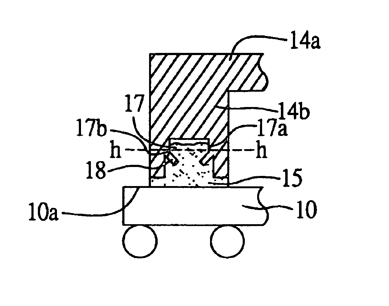
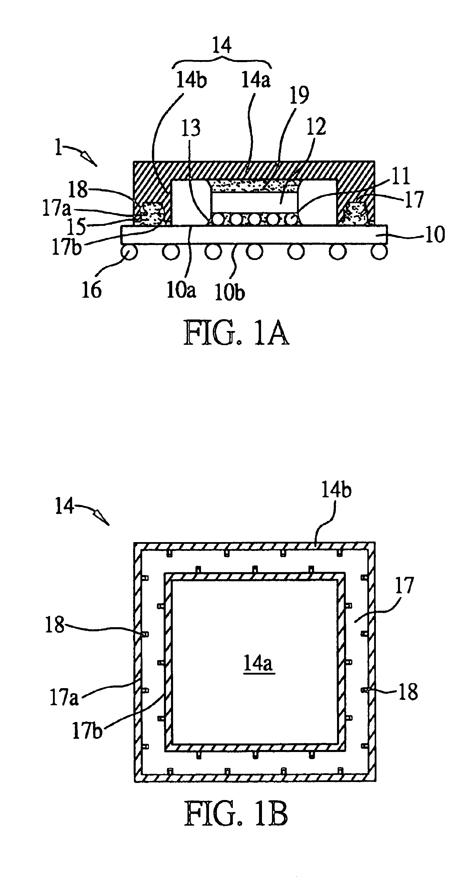
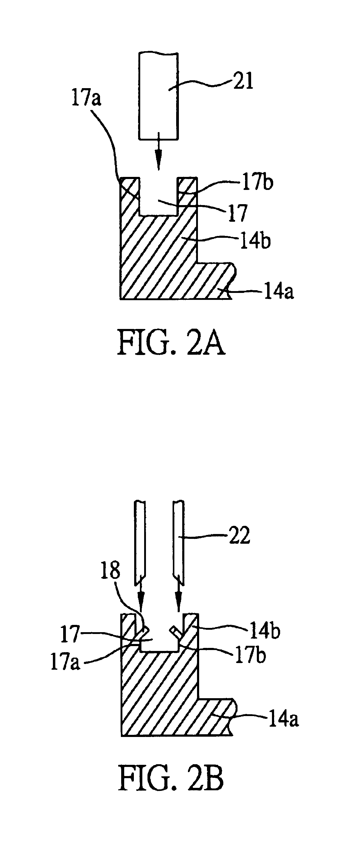
Preferred embodiments of a semiconductor package with a heat sink according to the present invention are described in detail with references to FIGS. 1 through 10.

FIGS. 1A and 1B show the semiconductor package 1 according to a preferred embodiment of the invention. As shown in the drawings, this semiconductor package 1 uses a substrate 10 as a chip carrier primarily made of a conventional resin material such as epoxy resin, polyimide resin, BT (Bismaleimide Triazine) resin, FR4 resin, etc.

The substrate 10 has a top surface 10a and a bottom surface 10b. The top surface 10a of the substrate 10 is formed with a plurality of bond pads (not shown) at predetermined positions where solder bumps 11 are bonded, and the bottom surface 10b of the substrate 10 is formed with a plurality of ball pads (not shown) for being implanted with solder baits 16. The substrate 10 is fabricated by conventional processes that are not to be further detailed herein.

At least one chip 12 is prepared, having an ...


PUM


Abstract

A semiconductor package includes a substrate having a top surface and a bottom surface; at least one chip mounted on the top surface of the substrate and electrically connected to the substrate; a heat sink attached to the top surface of the substrate by an adhesive material applied therebetween; and a plurality of solder balls implanted on the bottom surface of the substrate. The heat sink has a flat portion and a support portion connected to the flat portion. The support portion has at least one recess portion facing toward the top surface of the substrate and at least one burr formed on an interior surface of the recess portion such that the adhesive material can fill the recess portion and submerge the burr to provide an anchoring effect to firmly secure the heat sink in position on the substrate.

Description

FIELD OF THE INVENTIONThe present invention relates to semiconductor packages, and more particularly, to a semiconductor package with a heat sink for improving heat dissipating efficiency of the semiconductor package.BACKGROUND OF THE INVENTIONA FCBGA (flip-chip ball grid array) semiconductor package is formed with both a flip-chip structure and a ball grid array in which at least one chip is mounted and electrically connected to a surface of a substrate by a plurality of solder bumps, and a plurality of solder balls are implanted on an opposite surface of the substrate to serve as input / output (I / O) connections of the semiconductor package. In order to dissipate heat produced from operation of the chip, a heat sink is usually incorporated in the semiconductor package, as disclosed by U.S. Pat. Nos. 5,311,402, 5,637,920, 5,931,222 and 6,011,304. This heat sink is attached to the substrate by means of an adhesive or solder and is usually greater in surface area than the chip, such th...

Claims


Application Information

Patent Timeline
Patent Type & Authority Patents(United States)
IPC IPC(8): H01L21/02H01L23/367H01L21/48H01L23/34
CPCH01L21/4882H01L23/367H01L2224/16225H01L2224/73253H01L2924/15311H01L2224/32245H01L2924/16315H01L2224/32225H01L2224/73204H01L2924/16251H01L2924/16152H01L2924/00012H01L2224/72H01L2924/00015
Inventor HUANG, CHIEN-PINGHSIAO, CHENG-HSUCHIU, SHIH-KUANG
Owner SILICONWARE PRECISION IND CO LTD
Why Eureka
Try Eureka