Structure and method for biasing phase change memory array for reliable writing

Active Publication Date: 2006-07-20
SANDISK TECH LLC
View PDF18 Cites 354 Cited by
  • Summary
  • Abstract
  • Description
  • Claims
  • Application Information

AI Technical Summary

Benefits of technology

[0007] The present invention is defined by the appended claims, and nothing in this section should be taken as a limitation on those claims. In general, the invention is directed to methods of programming an array of nonvolatile memory cells each comprising a phase change element in series with a diode. Th

Problems solved by technology

This problem becomes increasingly important as operating voltages are decreased, write speeds are increased, memory cell densities are increased, and array sizes are increased.
One problem when writing and reading memories is that switching occurs very fast, and sometimes a word line or

Method used


Image

  • Structure and method for biasing phase change memory array for reliable writing
  • Structure and method for biasing phase change memory array for reliable writing
  • Structure and method for biasing phase change memory array for reliable writing

Examples


Embodiment Construction

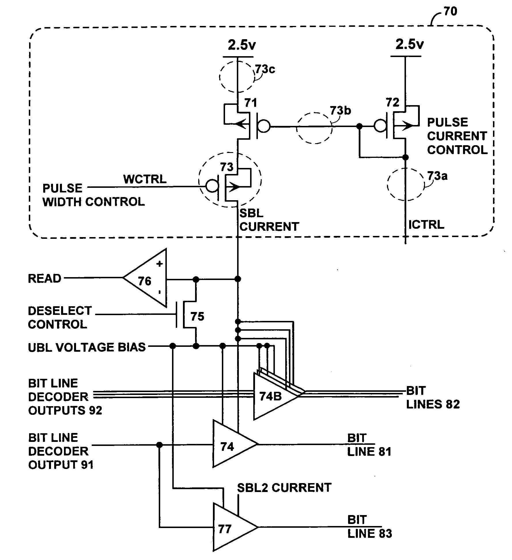
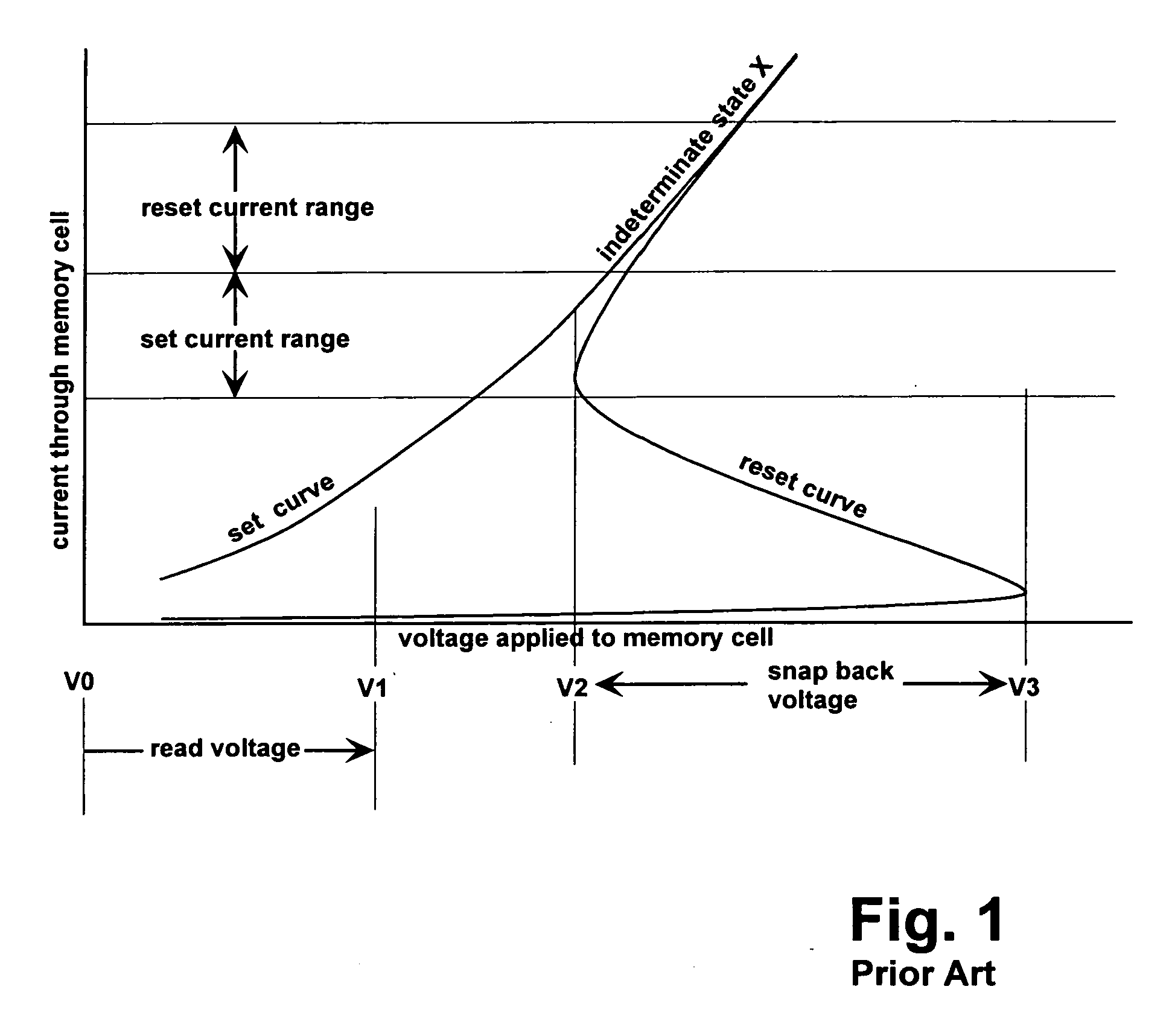
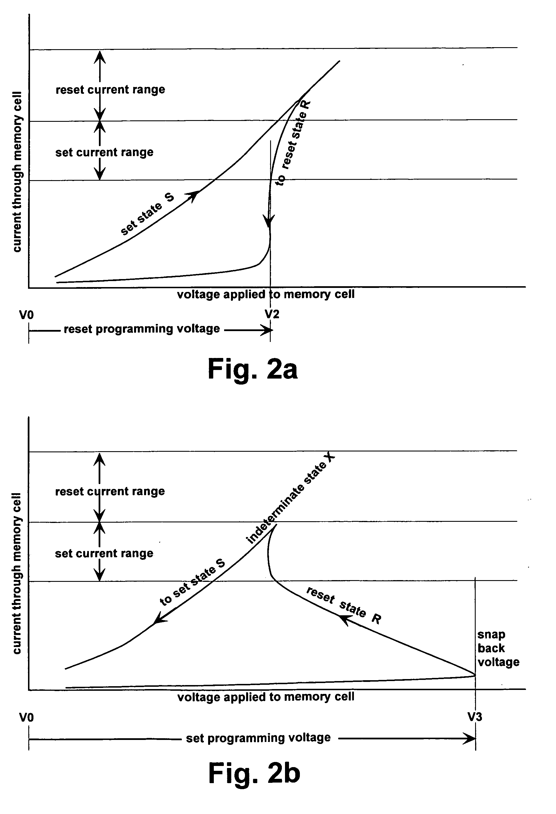
[0023] While many solid materials can change between crystalline and amorphous states, in this discussion the term “phase change material” will be used to describe a material that changes relatively easily from one stable state to another. The change is typically from an amorphous state to a crystalline state or vice versa, but may include an intermediate change, such as from a more ordered crystalline state to an indeterminate state to an amorphous state, or vice versa. Phase change material is converted from one state to the other by heating to high temperature, then cooling at a selected rate. Chalcogenides are well-known phase change materials.

[0024] It is known to use phase change materials, such as chalcogenides, in a nonvolatile memory cell, in which a high-resistance, amorphous state represents one memory state while a low-resistance, crystalline state represents the other memory state, where memory states correspond to values of 1 and 0. (If intermediate stable states are ...


PUM


Abstract

A memory array having memory cells comprising a diode and a phase change material is reliably programmed by maintaining all unselected memory cells in a reverse biased state. Thus leakage is low and assurance is high that no unselected memory cells are disturbed. In order to avoid disturbing unselected memory cells during sequential writing, previously selected word and bit lines are brought to their unselected voltages before new bit lines and word lines are selected. A modified current mirror structure controls state switching of the phase change material.

Description

RELATED APPLICATIONS [0001] This application relates to Herner et al., U.S. patent application Ser. No. 10 / 855,784, “An Improved Method for Making High-Density Nonvolatile Memory,” filed May 26, 2004; which is a continuation of Herner et al., U.S. patent application Ser. No. 10 / 326,470, “An Improved Method for Making High-Density Nonvolatile Memory,” filed Dec. 19, 2002 (since abandoned) and hereinafter the '470 application, both assigned to the assignee of the present invention and hereby incorporated by reference in their entirety. [0002] This application also relates to Scheuerlein et al, U.S. application Ser. No. ______, (attorney docket number MA-086-a-3) entitled “A Non-Volatile Memory Cell Comprising a Dielectric Layer and a Phase Change Material in Series”; to Scheuerlein, U.S. application Ser. No. ______, (attorney docket number MA-133) entitled “A Non-Volatile Phase Change Memory Cell Having a Reduced Thermal Contact Area”; and to Scheuerlein, U.S. application Ser. No.____...

Claims


Application Information

Patent Timeline
IPC IPC(8): H01L29/02
CPCG11C13/0004G11C13/0038G11C13/0069G11C2013/009G11C2213/72G11C11/21H01L27/2409H01L27/2463H01L27/2481G11C13/0023G11C2213/71H10B63/20H10B63/80H10B63/84G11C13/02G11C5/14
Inventor SCHEUERLEIN, ROY E.
Owner SANDISK TECH LLC
Why Eureka
Try Eureka