Capacitance detecting circuit and method, and fingerprint sensor using the same

a capacitance detection and circuit technology, applied in the field of capacitance detection circuit and method, fingerprint sensor using the same, can solve the problems of inability to completely eliminate the external disturbance noise caused by the above-described beat components, the inability to precisely detect the capacitance change due to external disturbance noise, and the influence of external disturbance noise superposed on the row lines can be relatively reduced, so as to improve the detection sensitivity. , the effect of improving the detection sensitivity

Active Publication Date: 2006-07-20
SYNAPTICS INC
View PDF2 Cites 77 Cited by
  • Summary
  • Abstract
  • Description
  • Claims
  • Application Information

AI Technical Summary

Benefits of technology

[0019] Accordingly, in view of the above-described background, it is an object of the present invention to provide a capacitance detecting circuit and method in which the influence of external disturbance noise can be suppressed to improve the S / N ratio so that very small capacitances Cs and capacitance changes ΔCs of the capacitances Cs at intersections (sensor devices) between row lines and column lines can be detected at a sufficient sensitivity level, and also to provide a fingerprint sensor using the above-described capacitance detecting circuit and method.

Problems solved by technology

Thus, in the capacitor detecting circuits, conducted noise transmitted to the capacitor sensor via a power supply or a human body is superposed on signals in the row lines and the column lines, thereby making it difficult to precisely detect a capacitance change due to this external disturbance noise.
In inverted fluorescent light, which is mainly used as current fluorescent light, a fluorescent lamp is switched ON by generating high frequencies by using semiconductors, causing noise having a fundamental frequency at a several dozens of KHz range.
Thus, when using a fingerprint sensor, if a device including a noise source having a frequency close to the sampling frequency of the capacitor detecting circuit, for example, the above-described inverted fluorescent light, is placed near the user, or if the fingerprint sensor is connected to a device having an inverter circuit used in backlight of a liquid crystal device, external disturbance noise caused by the above-described beat components cannot be completely eliminated.
Accordingly, the signal-to-noise (S / N) ratio for detecting capacitance changes is reduced, thereby making it difficult to precisely read the fingerprint of the user.

Method used


Image

  • Capacitance detecting circuit and method, and fingerprint sensor using the same
  • Capacitance detecting circuit and method, and fingerprint sensor using the same
  • Capacitance detecting circuit and method, and fingerprint sensor using the same

Examples


first embodiment

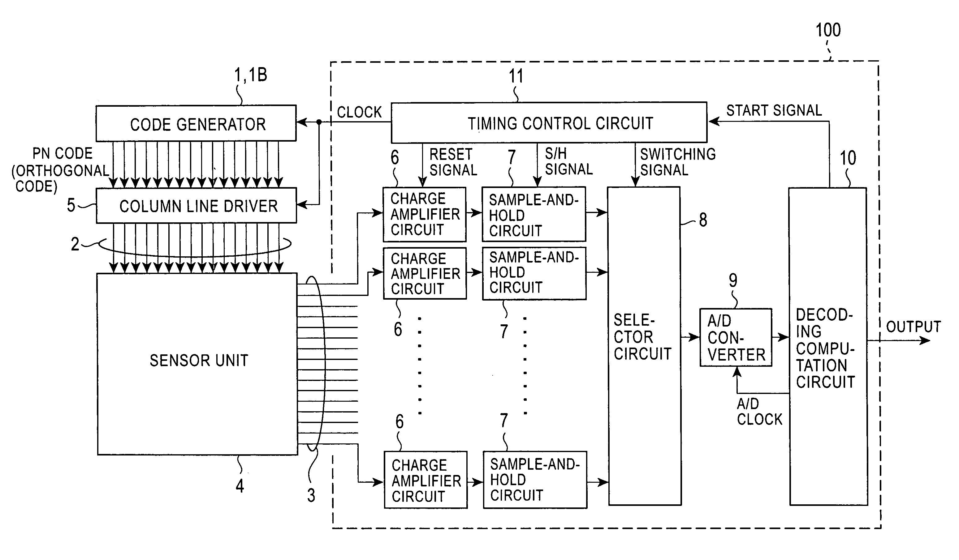
[0070] A capacitor detecting circuit constructed in accordance with a first embodiment of the present invention is discussed below with reference to FIG. 1.

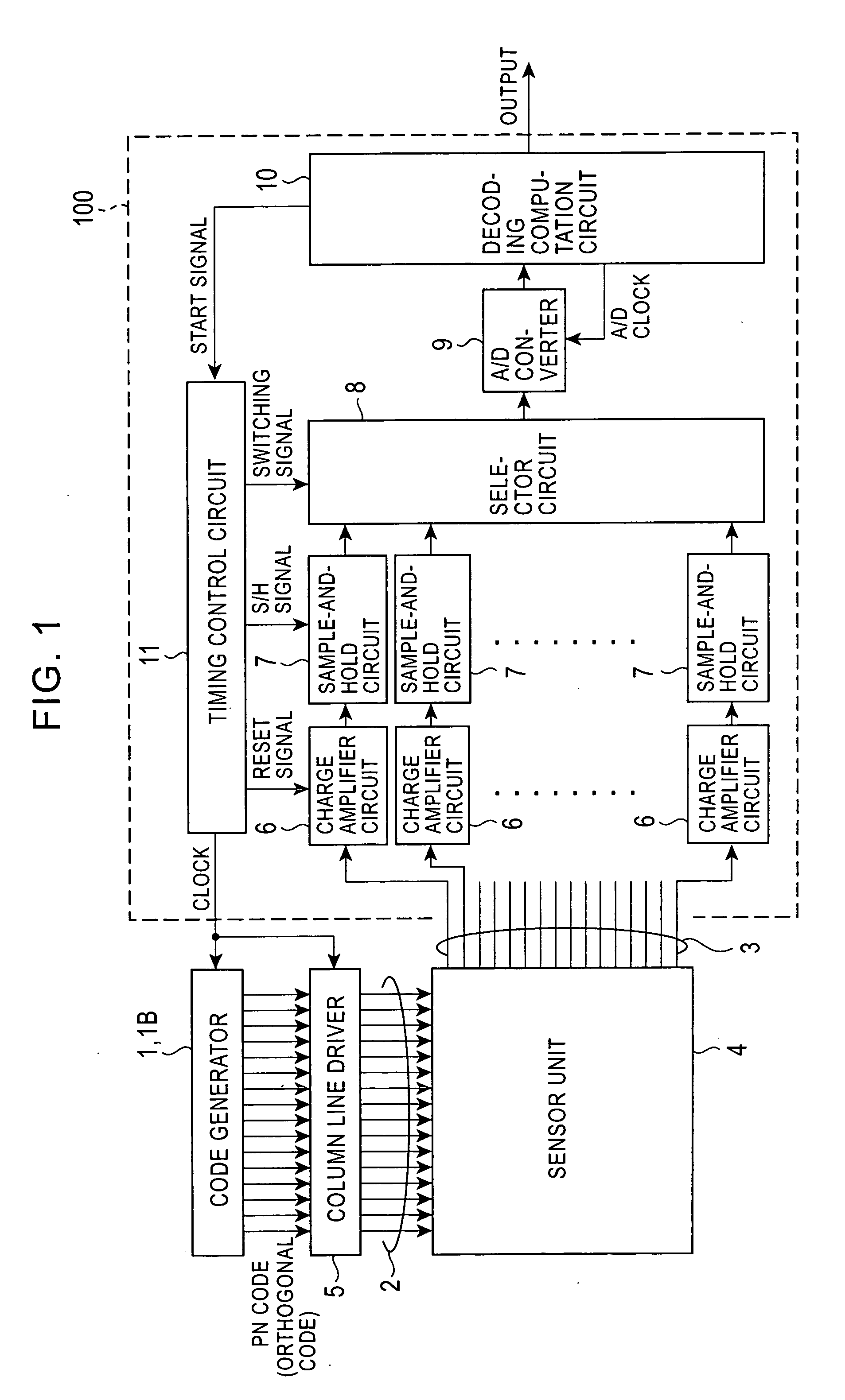
[0071] A code generator 1 generates pseudorandom noise (PN) code used for generating a column drive signal for driving the column lines of a column line set 2 of a sensor unit 4. As the PN code, M-series PN code having high autocorrelation is used. In the sensor unit 4, the column lines of the column line set 2 and row lines of a row line set 3 intersect with each other in a matrix, and the intersections form sensor devices (sensor devices 55 in FIG. 4).

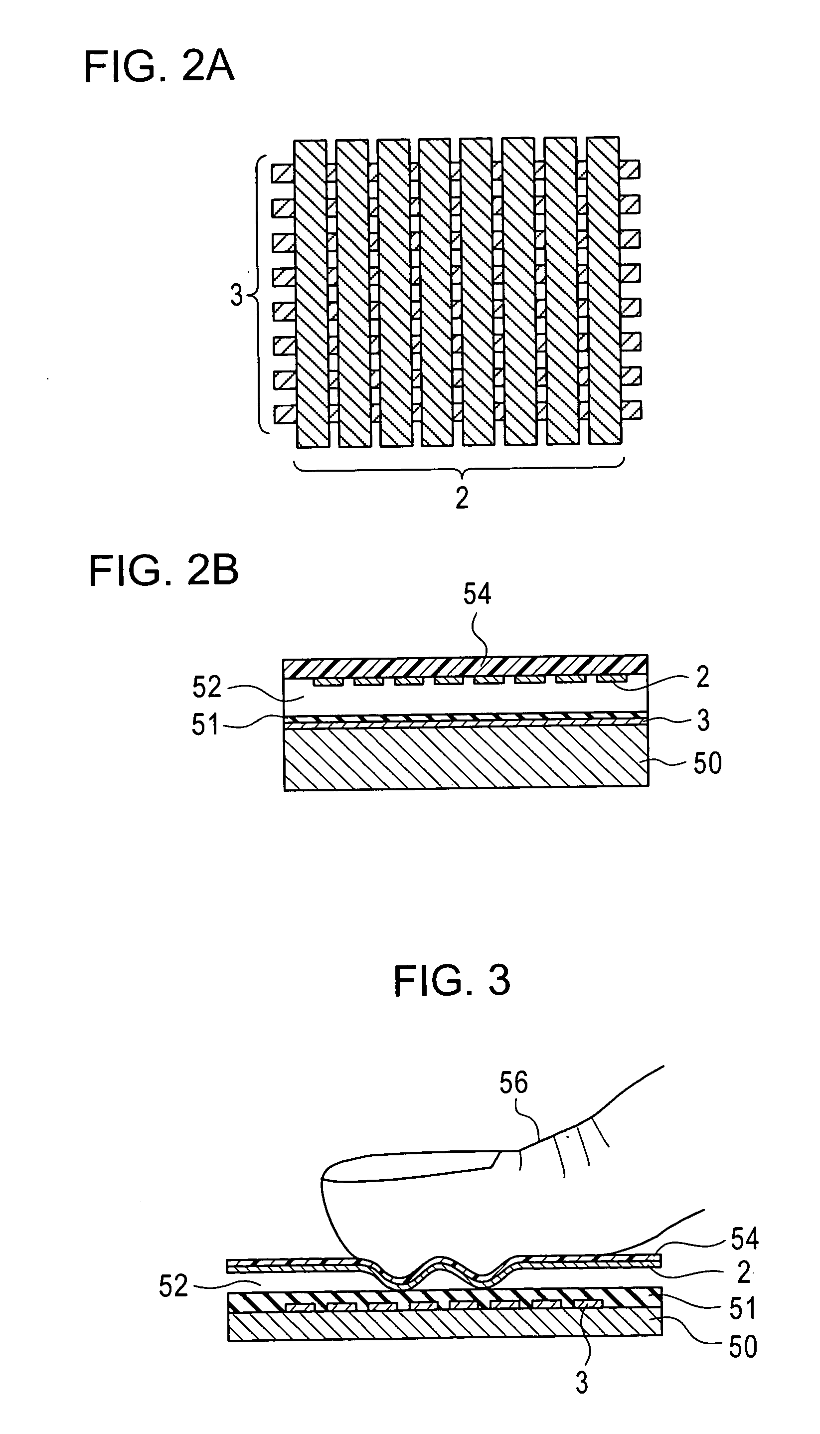
[0072]FIGS. 2A and 2B are a plan view and a sectional view, respectively, illustrating the sensor unit 4. As shown in FIG. 2A, the row lines of the row line set 3 and the column lines of a column line set 2 intersect with each other at a pitch of, for example, 50 μm. As shown in FIG. 2B, the row line set 3 consisting of a plurality or row lines are disposed on a substrate 50. An...

second embodiment

[0189] A capacitance detecting circuit constructed in accordance with a second embodiment of the present invention is described below with reference to FIG. 1. Elements similar to those of the first embodiment are designated with like reference numerals, and an explanation thereof is thus omitted.

[0190] The capacitance detecting circuit of the second embodiment differs from that of the first embodiment in that the code generator 1 for generating PN code is substituted with a code generator 1B for generating orthogonal code.

[0191] The code generator 1B generates orthogonal code used for generating a control signal for selecting the row lines of the row line set 3 of the sensor unit 4. As the orthogonal code, orthogonal code having high orthogonality, for example, Walsh code, is used.

[0192] That is, as in the code generator 1, the code generator 1B divides the column line set 2 into two column line groups, i.e., the first column line group and the second column line group, based on...

third embodiment

[0248] A capacitance detecting circuit constructed in accordance with a third embodiment of the present invention is described below with reference to FIG. 27. Elements corresponding to those of the first and second embodiments are designated with like reference numerals, and an explanation thereof is thus omitted.

[0249] The third embodiment differs from the first and second embodiments in that the columns lines of the column line set 2 are divided into a plurality of column line groups, and the column line groups are sequentially selected one by one to perform multiplexing measurements, namely, while a selected column line group performs measurements, the other (unselected) column line groups do not perform measurements.

[0250] In other words, in the first and second embodiments, multiplexing by using the PN code or orthogonal code is performed on the overall column lines, while in the third embodiment, column lines are complementarily driven in each of the column line groups so a...


PUM


Abstract

In a capacitance detecting circuit, changes in capacitances at intersections between a plurality of column lines and a row line are detected as voltages. The capacitance detecting circuit includes a code generator for generating code having orthogonality in chronological order. A column-line driver drives the plurality of column lines based on the code by dividing the column lines into a first column line group and a second column line group. A capacitance detector, which is connected to the row line, converts the total of currents generated in capacitances at the intersections with the driven column lines into a voltage signal and outputs the converted voltage signal. A decoding computation unit determines the voltages corresponding to the capacitances at the intersections for each of the column line groups by performing product sum computation between the measured voltages and the code. In a period for detecting the capacitances, the column-line driver drives the first column line group and the second column line group by complementary voltages according to the code or information indicating the inversion of the code.

Description

BACKGROUND OF THE INVENTION [0001] 1. Field of the Invention [0002] The present invention relates to a capacitance detecting circuit and method for detecting a very small capacitance, and also to a fingerprint sensor using the same. [0003] 2. Description of the Related Art [0004] As a known fingerprint sensor, which is considered to be most promising in biometrics techniques, the following type of pressure-sensitive capacitance sensor has been developed. Row lines and column lines are formed at predetermined intervals on the surfaces of two films, and the two films are disposed with a predetermined gap therebetween such that they face each other with an insulating film therebetween. [0005] In this pressure-sensitive capacitance sensor, when a finger is placed on the sensor, the shape of the films are changed according to the ridges and valleys of the fingerprint, and accordingly, the intervals between the row lines and the column lines are changed. Thus, the shape of the fingerprint...

Claims


Application Information

Patent Timeline
Patent Type & Authority Applications(United States)
IPC IPC(8): G01R27/26G06K9/00A61B5/117G06T1/00
CPCG06F3/0446G06F3/04182G06V40/1306
Inventor UMEDA, YUICHISAITO, JUNICHI
Owner SYNAPTICS INC
Why Eureka
Try Eureka