

Apparatus and method for independent control of on-die termination for ouput buffers of a memory device
a memory device and on-die termination technology, which is applied in the direction of digital storage, instruments, and increasing the degree of modification, can solve the problems of negative impact on the performance of the memory device, the time difference at which a signal is received along the length of the signal line, and the timing skew between the signals that are provided
- Summary
- Abstract
- Description
- Claims
- Application Information
AI Technical Summary
Benefits of technology
Problems solved by technology
Method used
Image

Examples
Embodiment Construction
[0022] Certain details are set forth below to provide a sufficient understanding of the invention. However, it will be clear to one skilled in the art that the invention may be practiced without these particular details. In other instances, well-known circuits, control signals, timing protocols, and software operations have not been shown in detail in order to avoid unnecessarily obscuring the invention.
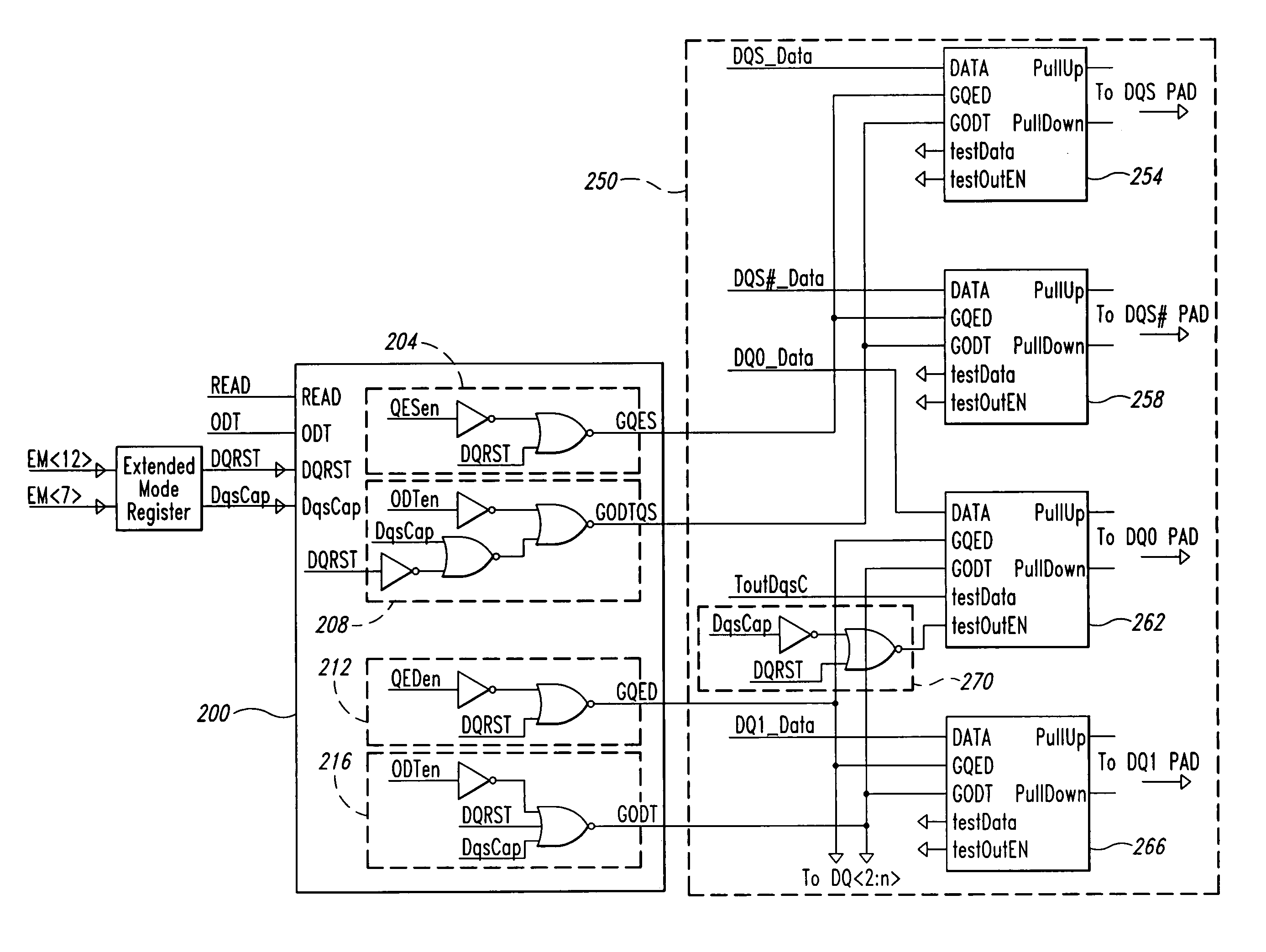
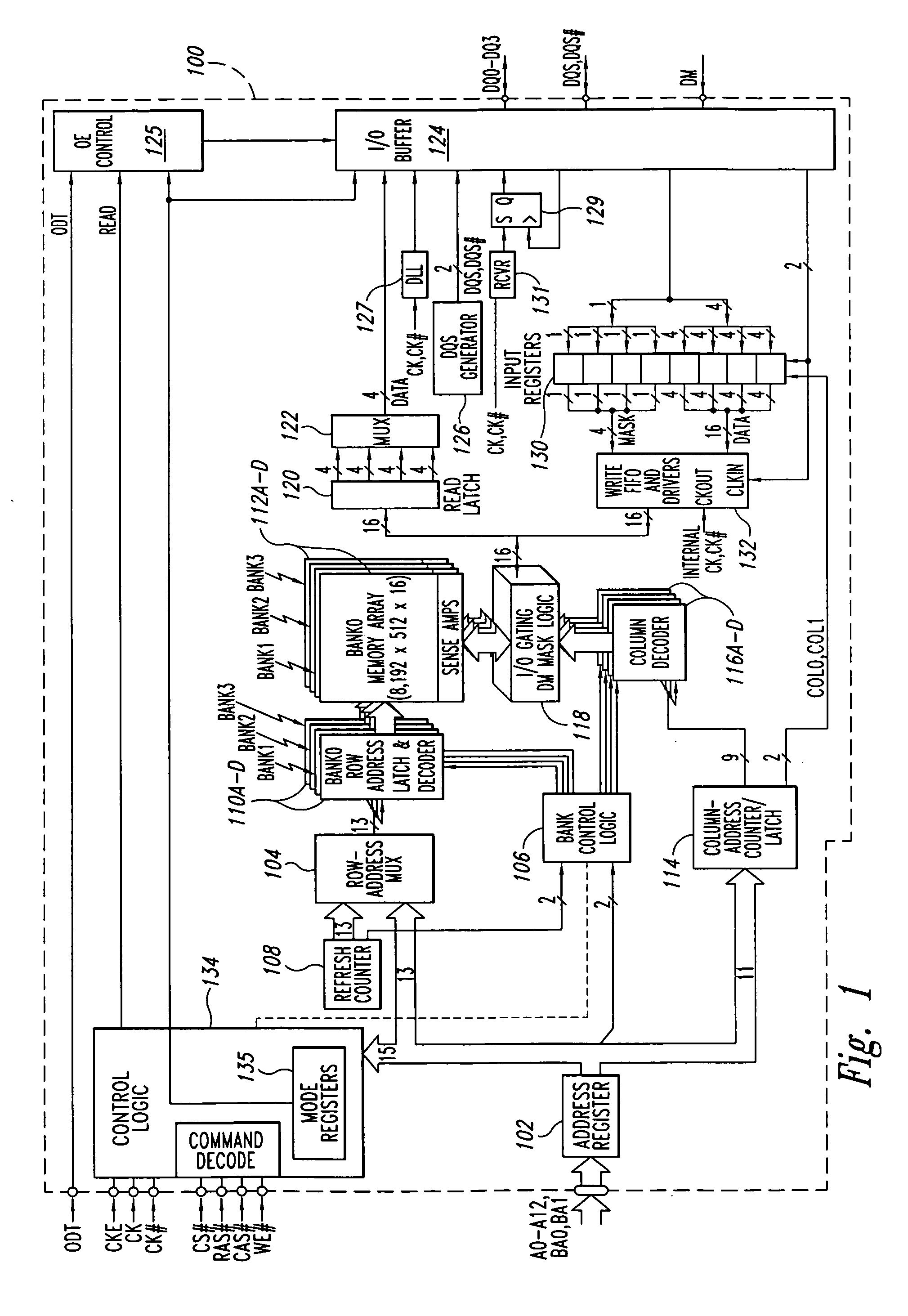
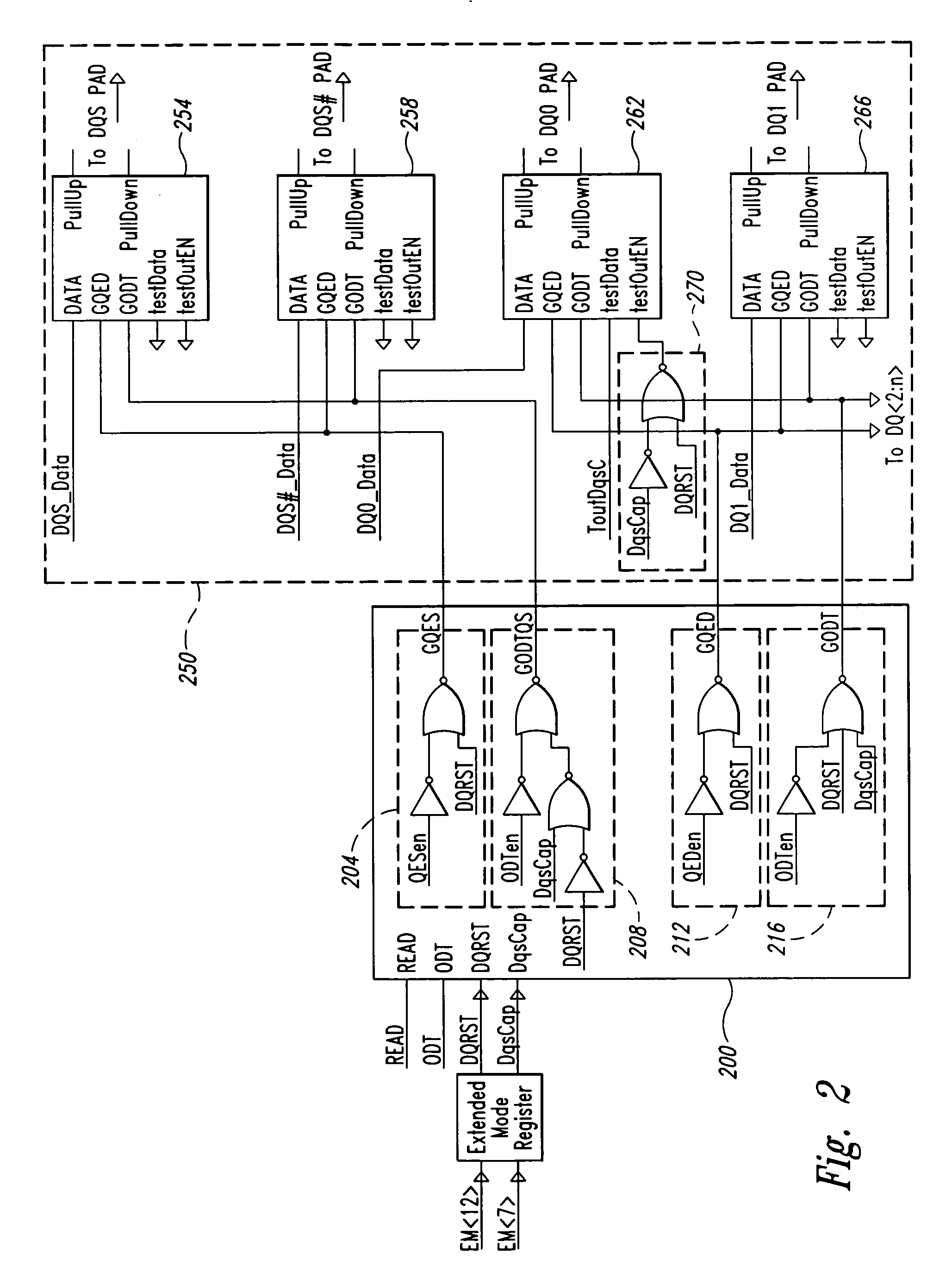
[0023]FIG. 1 illustrates a memory device in which an embodiment of the present invention is implemented. The memory device 100 in FIG. 1 is a double-data rate (DDR) synchronous dynamic random access memory (“SDRAM”). The memory device 100 is referred to as a double-data-rate device because the data words DQ being transferred to and from the device are transferred at double the rate of a conventional SDRAM, which transfers data at a rate corresponding to the frequency of the applied clock signal. However, the principles described herein are applicable to any memory device that may in...
PUM
 Abstract
Description
Claims
Application Information