Exposure equipment and control method of the same

a technology of exposure equipment and control method, which is applied in the direction of printers, semiconductor/solid-state device details, instruments, etc., can solve the problems of unacceptable effect, unignorable, and extremely long exposure time of wafers, and achieves high reliability, prevents deterioration of resists, and suppresses line width fluctuation of patterns

Active Publication Date: 2006-07-20
FUJITSU LTD
View PDF3 Cites 5 Cited by
  • Summary
  • Abstract
  • Description
  • Claims
  • Application Information

AI Technical Summary

Benefits of technology

[0010] The present invention has been made in view of the above-described problems, and an object thereof is to provide, in a lithography system in which an exposure equipment and the other equipment are separately installed, an exposure equipment capable of suppressing a line width fluctuation of a pattern by preventing deterioration of a resist, and of realizing a highly reliable exposure that can enough respond to a further microfabrication of the patterns, even if a processing for a wafer takes an extremely long time as in an electron-beam exposure, and a controlling method thereof.

Problems solved by technology

In the case of an electron-beam exposure, in particular, the exposure for wafer takes an extremely long time.
Depending on the waiting time, a reaction between the resist and a base or the like shows a progress, exercising an unacceptable effect on a line width of a pattern to be formed.
Such a problem is becoming unignorable recently on the back of a progress in microfabrication of t he semiconductor elements, in which the allowable error range related to the line width is becoming smaller.
However, even with this technique, it is extremely difficult to suppress the line width fluctuation of the pattern, once the resist suffers deterioration caused by a long-time exposure to the airflow.

Method used


Image

  • Exposure equipment and control method of the same
  • Exposure equipment and control method of the same
  • Exposure equipment and control method of the same

Examples


first embodiment

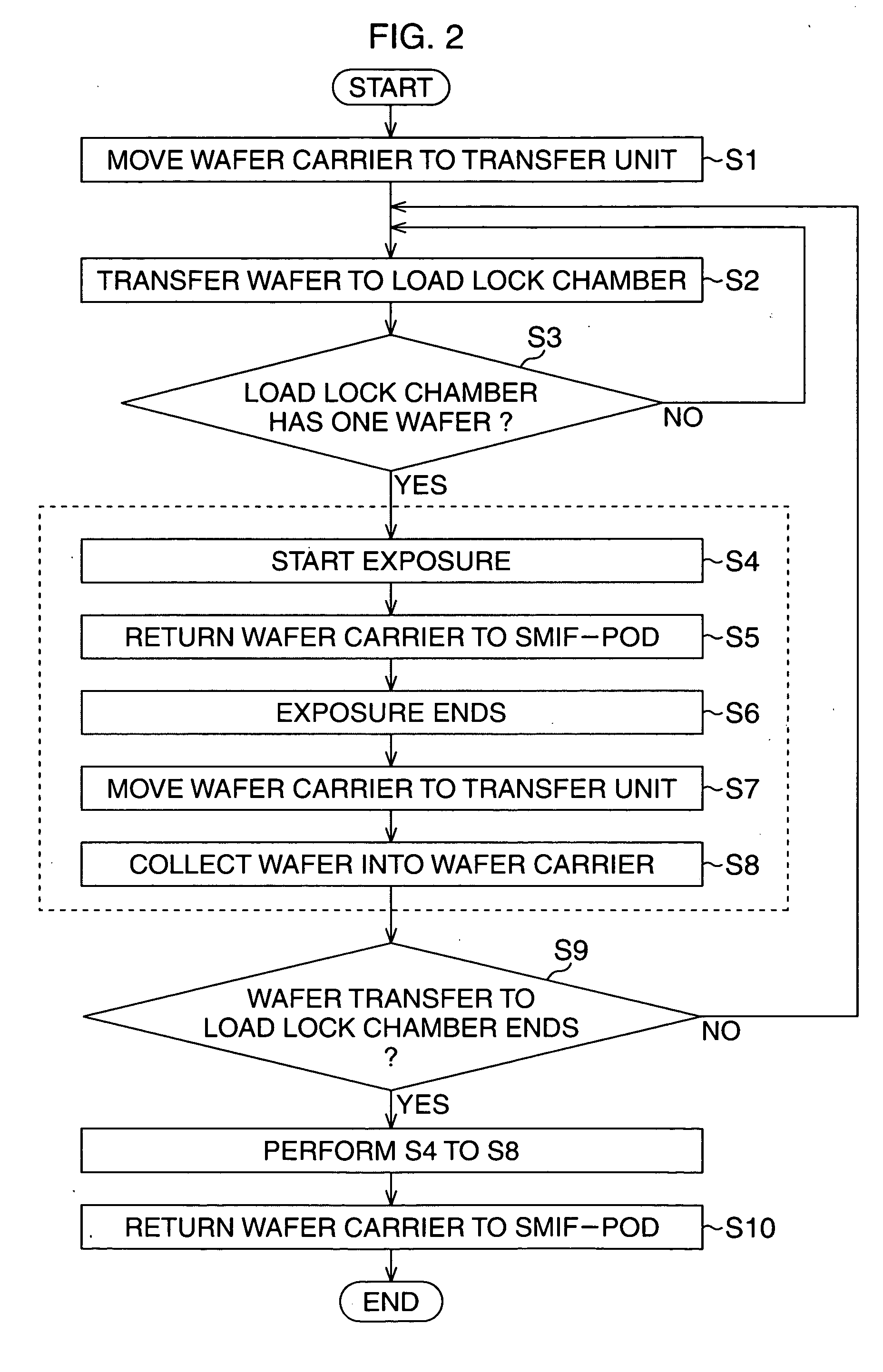
[0028] [Basic Configuration of Electron-Beam Exposure Equipment]

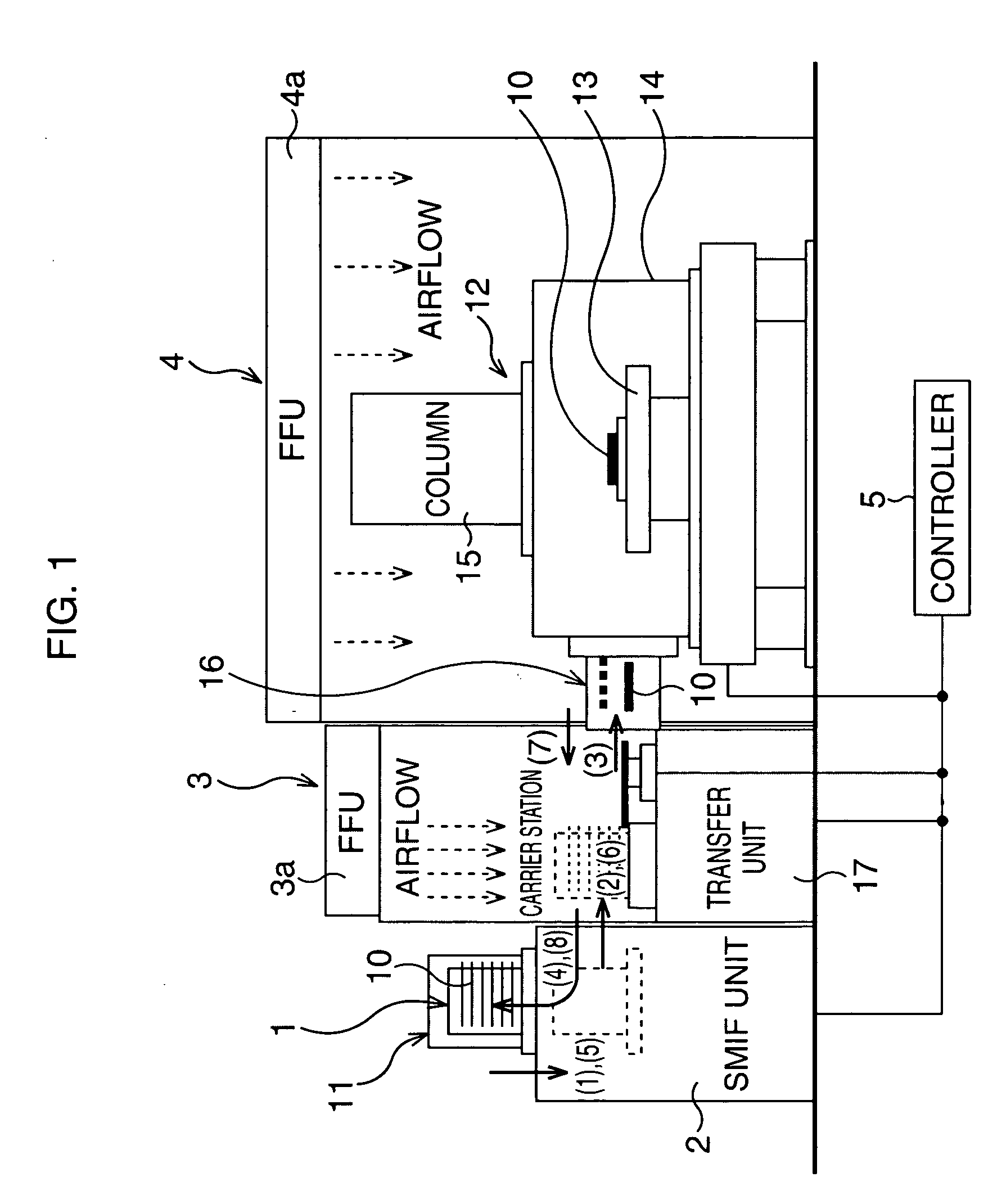
[0029]FIG. 1 is a schematic view showing an electron-beam exposure equipment with a SMIF unit according to a first embodiment.

[0030] The electron-beam exposure equipment according to the present embodiment is configured to include a wafer carrier 1 containing wafers being subject to exposure, in this case, semiconductor wafers 10, a SMIF unit 2, an equipment body 12 exposing the wafer 10, a transfer area 3 provided between the SMIF unit 2 and the thermal chamber 4 to be a transfer path of the wafers 10, a controller 5 controlling a transfer operation or the like of the wafer carrier 1 and the wafers 10.

[0031] The wafer carrier 1 is designed to contain two or more wafers 10 and be movable between the SMIF unit 2 and the thermal chamber 4 or the other equipment via the transfer area 3.

[0032] The SMIF unit 2 includes a SMIF-POD 11 containing the wafer carrier 1 in an attachable / detachable manner. The wafer carrier 1 det...

second embodiment

[0058] [Basic Configuration of Electron-Beam Exposure Equipment]

[0059]FIG. 3 is a schematic view showing a schematic configuration of an electron-beam exposure equipment with a SMIF unit according to a second embodiment. Here, the same component or so forth as of the electron-beam exposure equipment according to the first embodiment will be denoted by the same numerical reference and the description thereof will be omitted. The electron-beam exposure equipment according to the present embodiment is configured to include a protection plate 21 for the wafer carrier 1 and a protection plate arrangement mechanism 22 in the transfer area 3 in addition to the respective components shown in FIG. 1.

[0060] The protection plate 21 is to shield the containable plural wafers in the wafer carrier 1 against the airflow generated by the FFU 3a when the wafer carrier 1 is sent to the transfer unit 17 by the controller 5, for example, when the wafer 10 is exposed. An a specific example of the prote...

third embodiment

[0082] In a third embodiment, a combined configuration of the above-described first and second embodiments will be disclosed.

[0083] The schematic configuration of the electron-beam exposure equipment according to the present embodiment is the same as that in FIG. 3 (and FIG. 4).

[0084] [Basic Operation of Electron-Beam Exposure Equipment]

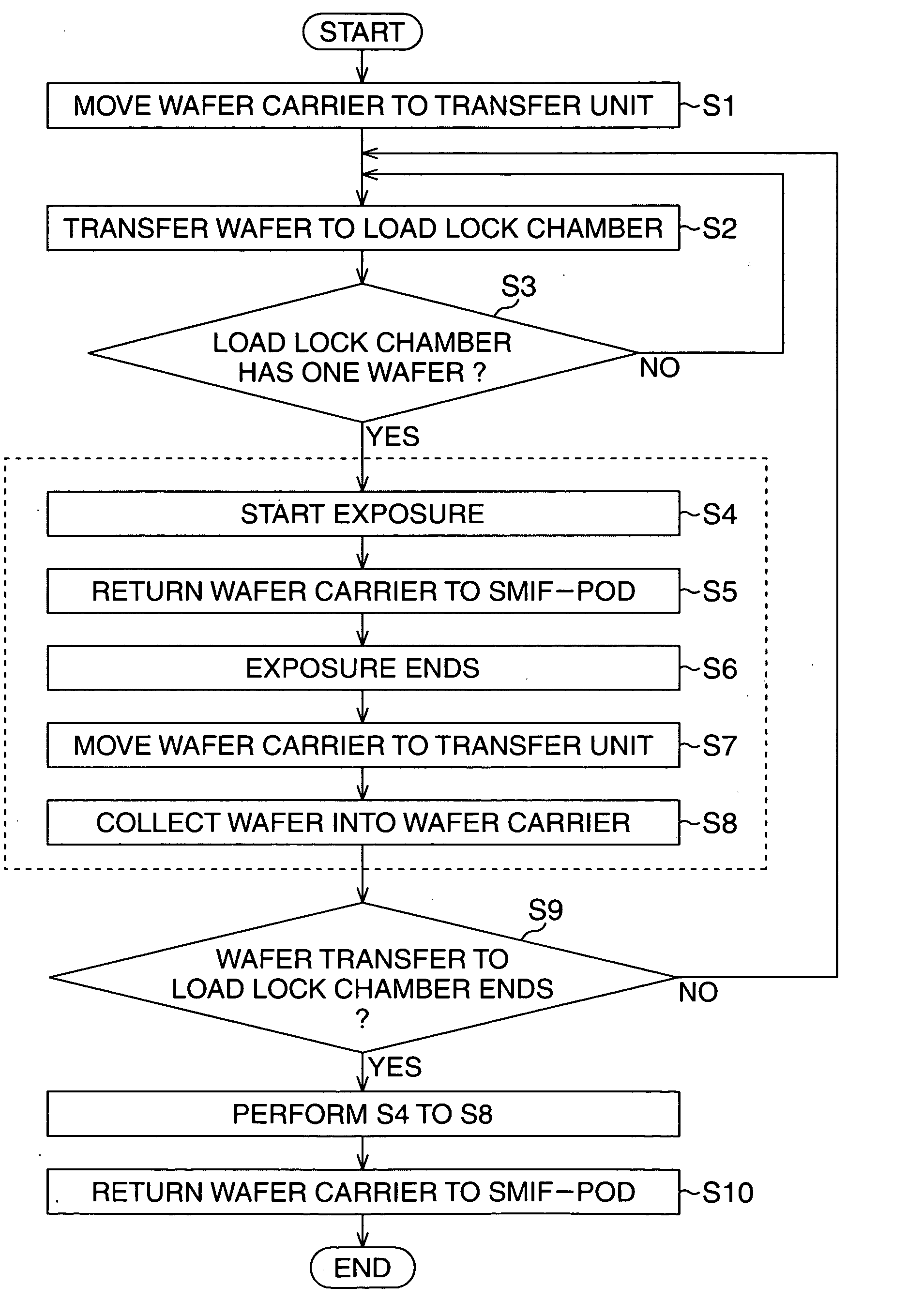
[0085]FIG. 7 is a float chart showing a basic operation of an exposure equipment with a SMIF unit according to the third embodiment.

[0086] In the electron-beam exposure equipment according to the present embodiment, a basic operation including transfer, collection, and exposure of the wafer 10, which will be described below, is placed under the control of the controller 5 and the protection plate arrangement mechanism 22.

[0087] First, the wafer carrier 1 containing plural wafers 10, each of which is coated with the resist on the surface thereof, is moved from the SMIF-POD 11 through inside the SMIF unit 2 into the space of the transfer unit 17 in...


PUM


Abstract

A controller controls a wafer carrier to move from a SMIF-POD to transfer and collect a wafer between a space of a transfer unit through a thermal chamber. The wafer carrier is returned into the SMIF-POD, when the wafer is exposed, to be kept waiting in the SMIF-POD until the wafer completes the exposure.

Description

CROSS-REFERENCE TO RELATED APPLICATIONS [0001] This application is based upon and claims the benefit of priority from the prior Japanese Patent Application No. 2005-007964, filed on Jan. 14, 2005, the entire contents of which are incorporated herein by reference. BACKGROUND OF THE INVENTION [0002] 1. Field of the Invention [0003] The present invention relates to an exposure equipment to fabricate a semiconductor element, a magnetic head, or the like, and a controlling method of the same. [0004] 2. Description of the Related Art [0005] Conventionally, when fabricating a semiconductor element, a magnetic head, or the like, a lithography technology has been in use, in which a predetermined pattern is transferred onto a resist coated on a wafer surface by an exposure to light. As a system configuration to perform an exposure using a beam such as ultraviolet or laser as a lithography process, there is a lithography system of a so-called inline type, in which a resist coating equipment, e...

Claims


Application Information

Patent Timeline
Patent Type & Authority Applications(United States)
IPC IPC(8): H01L21/50H01L23/02
CPCH01L21/67225H01L21/67745
Inventor YAMADA, KEIJI
Owner FUJITSU LTD
Why Eureka
Try Eureka