Phase change memory and fabricating method thereof

a phase change and memory technology, applied in the field of phase change memory, can solve the problems of increasing the difficulty of controlling the whole process, increasing the difficulty of the subsequent process, and large changes in the manufacturing process, so as to achieve the effect of not increasing the difficulty of the manufacturing process

Inactive Publication Date: 2006-07-27
IND TECH RES INST
View PDF10 Cites 20 Cited by
  • Summary
  • Abstract
  • Description
  • Claims
  • Application Information

AI Technical Summary

Benefits of technology

[0019] According to the embodiment, the manufacturing process does not need modification for the disclosed phase change memory, thus the difficulty of the manufacturing process is not increased.
[0020] In the following description, for purposes of explanation, numerous specific details are set forth in order to provide a thorough understanding of the invention. It will be apparent, however, to one skilled in the art that the invention can be practiced without these specific details. In other instances, structures and devices are shown in block diagram form in order to avoid obscuring the invention.

Problems solved by technology

However, the heating electrodes connect with the transistor, which provides limit currents; thus, reducing the write-in current for the phase change layer for phase transition has become the main development.
The approaches of the prior art face the problems of large changes in the manufacturing process or increasing difficulty in controlling the whole process.
However, difficulty is increased in the consequent process due to reducing of the thin film thickness by way of edge contact.
Besides, mask alignment greatly affects the contact areas of the edges.
Because it is difficult to reduce the width and the length of the electrodes simultaneously, the area of the memory cell may be reduced such that memory density is affected.
However, the technology disclosed in the prior art may not be easily integrated with the current process, which increases the difficulty in manufacturing.

Method used


Image

  • Phase change memory and fabricating method thereof
  • Phase change memory and fabricating method thereof
  • Phase change memory and fabricating method thereof

Examples


Embodiment Construction

[0028] Reference will now be made in greater detail to a preferred embodiment of the invention, an example of which is illustrated in the accompanying drawings. Wherever possible, the same reference numerals are used throughout the drawings and the description to refer to the same or like parts. Reference in the specification to “one embodiment” or “an embodiment” means that a particular feature, structure, or characteristic described in connection with the embodiment is included in at least one embodiment of the invention. The appearances of the phrase “in one embodiment” in various places in the specification are not necessarily all referring to the same embodiment.

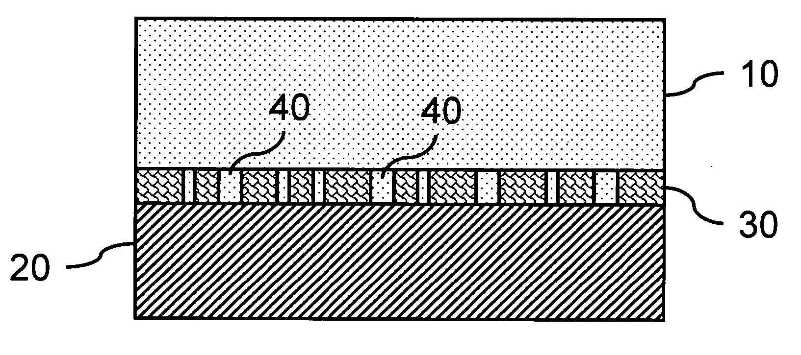
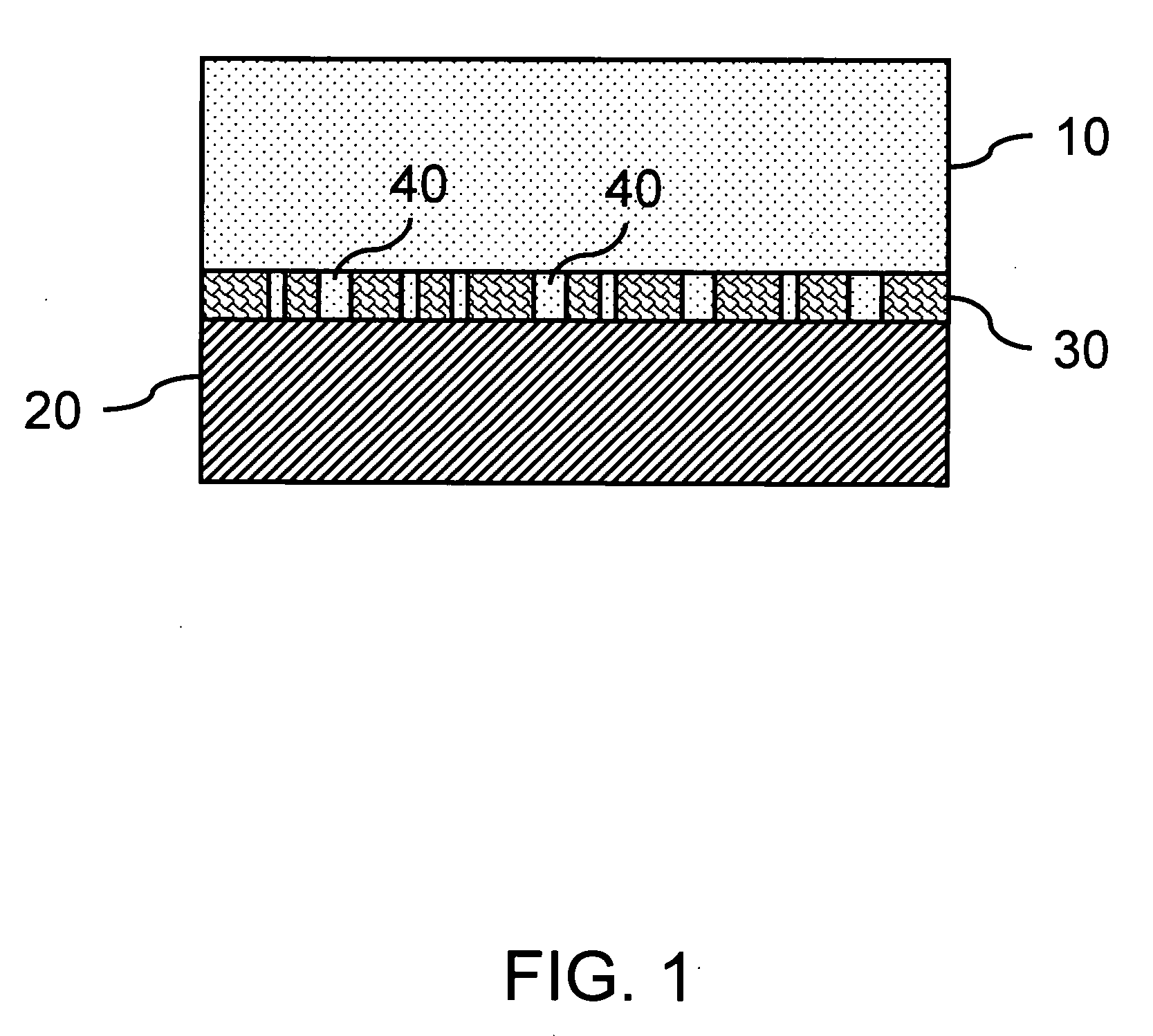
[0029]FIG. 1 illustrates one embodiment of the electrode structure of the phase change memory of the invention. FIG. 1 only shows a single memory (or memory cell). The actual MRAM array can be composed of several memories as shown in FIG. 1.

[0030] One surface of the phase change layer 10 is provided with an electrode ...


PUM


Abstract

A phase change memory including a phase change layer, a first electrode, and a porous dielectric layer formed with a plurality of pores. The porous dielectric layer is formed between the phase change layer and the first electrode. Therefore, the phase change layer may make contact with the first electrode thorough the pores thereby decreasing the contact areas of the phase change layer and the first electrode.

Description

[0001] This application claims the benefit of Taiwan Patent Application No. 94100497, filed on Jan. 7, 2005, which is hereby incorporated by reference for all purposes as if fully set forth herein. BACKGROUND [0002] 1. Field of Invention [0003] The invention relates to an electrode structure, and in particular to an electrode structure that is applicable for phase change memory to reduce the contact area between the electrode and the phase change layer for lowering the operation power and operation current. [0004] 2. Related Art [0005] Most electronic equipment uses different types of memories, such as DRAM, SRAM and Flash memory or a combination of these memories based on the requirements of the application, the operating speed, the memory size and the cost considerations of the equipment. The current developments in the memory technology field include FeRAM, MRAM and phase-change memory. Among the memories, phase-change memory will be mass manufactured in the future. [0006] The ph...

Claims


Application Information

Patent Timeline
Patent Type & Authority Applications(United States)
IPC IPC(8): H01L29/04
CPCH01L45/06H01L45/1233H01L45/1246H01L45/126H01L45/144H01L45/1666H10N70/828H10N70/8413H10N70/231H10N70/061H10N70/8828H10N70/826
Inventor LIANG, JIUH-MING
Owner IND TECH RES INST
Why Eureka
Try Eureka