
Eureka
For R&D, Eureka makes reading and utilizing patents & technical documents easy.
Eureka AIR
Designed for self-driven R&D workflows. Generate viable solutions, solve complex R&D challenges, empower your innovation with AI.

Eureka Materials
Designed for material experts only. Revolutionize your material R&D, from search, analyze, to developing new materials.

TechResearch
Generate reliable direction feasibility study reports for your R&D in just a few steps.

TechSeek
Discover and master advanced knowledge NOW. Basics, ideas, possibilities, all at once.

TechMind
As an expert in R&D Theories, TechMind can generates customized viable solutions instantly.

TechRisk
Analyze your overall solution with one click, know your potential R&D risks in advance.

TechMonitor
Get weekly tech updates, stay abreast of the latest tech innovations and key insights.
Semiconductor device and method for manufacturing semiconductor device
- Summary
- Abstract
- Description
- Claims
- Application Information
AI Technical Summary
Benefits of technology
Problems solved by technology
Method used
Image

Examples
first embodiment
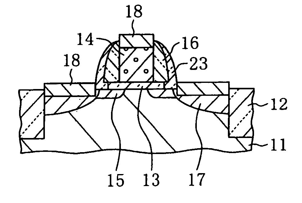
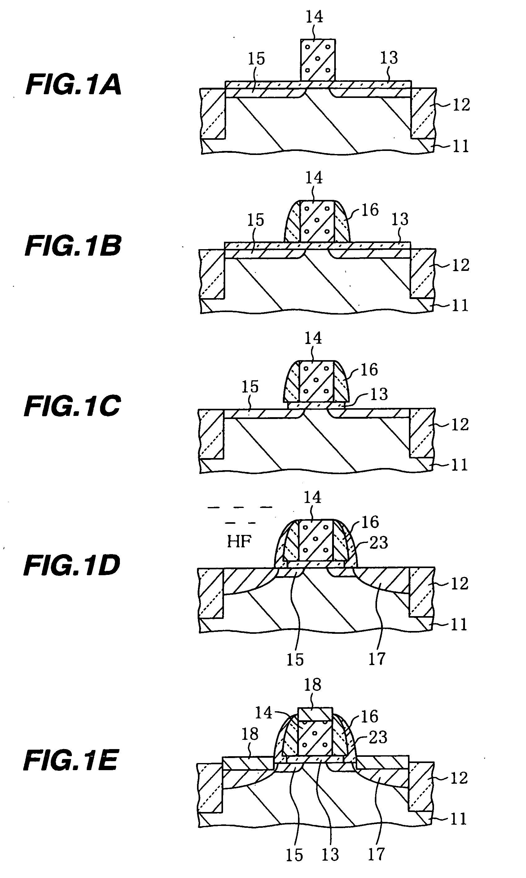
[0048] Embodiments of the present invention will be described with reference to the drawings. FIGS. 1A to 1E are cross sectional views schematically illustrating a manufacture method for a semiconductor device according to the present invention.
[0049] As shown in FIG. 1A, an isolation trench is formed in the surface layer of, e.g., a p-type semiconductor substrate 11, an insulating film is buried in the trench, and an unnecessary portion of the insulating film is removed by chemical mechanical polishing (CMP) to form an STI type isolation region 12. The surface of each active region defined by the isolation region 12 is thermally oxidized at 800° C. to 1100° C. to form a gate insulating film 13. A polysilicon film is deposited on the surface of the semiconductor substrate, covering the gate oxide film 13. By using a photoresist pattern as a mask, the polysilicon film is etched to pattern a gate electrode 14.
[0050] In this case, mixture gas of HBr and Cl2 is used as etching gas to p...
second embodiment
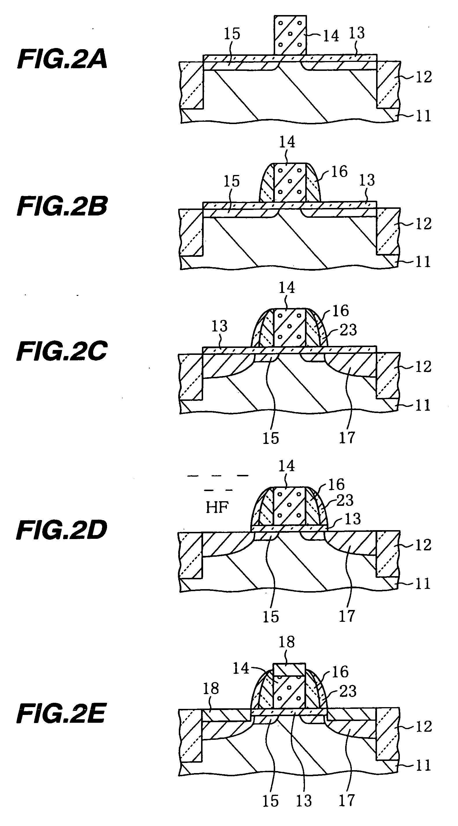
[0057]FIGS. 2A to 2E are cross sectional views schematically illustrating a semiconductor device manufacture method according to the present invention.
[0058]FIGS. 2A and 2B show the same structures as those shown in FIGS. 1A and 1B, and these structures can be manufactured by the same processes.
[0059] As shown in FIG. 2C, side wall spacers 23 of TEOS silicon oxide are formed covering the side wall spacers 16 of silicon nitride. The TEOS silicon oxide film has an etching rate faster than that of the thermally oxidized film. While the side wall spacers 23 are formed, control etching is performed to leave the gate oxide film 13.
[0060] As shown in FIG. 2D, for a silicidation reaction, the surfaces of the substrate 11 and gate electrode 14 are exposed by using dilute hydrofluoric acid solution. In this etching, the TEOS silicon oxide film 23 has an etching rate faster than that of the thermally oxidized gate oxide film 13. Therefore, when the gate oxide film 13 and TEOS silicon oxide f...
third embodiment
[0063]FIGS. 3A to 3E are cross sectional views schematically illustrating a semiconductor device manufacture method according to the present invention.
[0064]FIG. 3A shows the same structure as that shown in FIG. 1A, and this structure can be manufactured by the same process.
[0065] As shown in FIG. 3B, a silicon oxide film made of TEOS and a silicon nitride film are successively deposited covering the gate electrode 14, etched back to form laminated side wall spacers made of silicon oxide films 24 covering the side walls of the gate electrode 14 and silicon nitride films 16 on the silicon oxide films 24. Instead of the TEOS silicon oxide film, a silicon oxide film formed by thermal oxidation may be used. In forming the side wall spacers, the silicon nitride film is etched by using mainly CHF3 gas as etching gas, and the silicon oxide film is etched mainly by using CF4 gas as etching gas. If the gate oxide film 2 is to be left, control etching with limited time is performed.
[0066] A...
PUM
 Abstract
Description
Claims
Application Information
 - R&D Engineer
- R&D Manager
- IP Professional
- Industry Leading Data Capabilities
- Powerful AI technology
- Patent DNA Extraction
Browse by: Latest US Patents, China's latest patents, Technical Efficacy Thesaurus, Application Domain, Technology Topic, Popular Technical Reports.
© 2024 PatSnap. All rights reserved.Legal|Privacy policy|Modern Slavery Act Transparency Statement|Sitemap|About US| Contact US: help@patsnap.com