Defect analyzing device for semiconductor integrated circuits, system therefor, and detection method

a technology of defect analysis and integrated circuit, which is applied in the direction of measurement devices, semiconductor/solid-state device testing/measurement, instruments, etc., can solve the problems of large system structure, high cost of eb tester itself, and inability to analyze semiconductor devices and wiring boards in a small space. achieve the effect of improving manufacturing efficiency and yield

Inactive Publication Date: 2006-07-27
HITACHI LTD
View PDF3 Cites 36 Cited by
  • Summary
  • Abstract
  • Description
  • Claims
  • Application Information

AI Technical Summary

Benefits of technology

[0012] It is an object of the present invention to provide a compact semiconductor or wiring defect analysis apparatus capable of identifying a defective portion correctly.
[0013] It is another object of the present invention to provide a manufacture method for a semiconductor device or a wiring board capable of improving a manufacture efficiency and yield.

Problems solved by technology

It is therefore necessary to use a system capable of maintaining a vacuum state, resulting in a huge structure of the whole system.
There arises therefore a problem that a defect analysis of a semiconductor device and a wiring board cannot be made in a small space.
There is also another problem that an EB tester itself is very expensive.
However, if the irradiation current amount of an electron beam applied to a disconnection defect portion exceeds a threshold value, a state (irreversible charge-up) occurs in which the potential at a specimen surface does not recover the state without irradiation even if an electron beam irradiation is stopped, depending upon the type of a specimen, and resulting in a problem that a defect analysis cannot be made because of no change in a potential even if an electron beam is irradiated.
It is very difficult to control electron beam irradiation at a high precision in order to eliminate such a problem, i.e., in order to prevent the irreversible charge-up and obtain a clear displacement (flashing) potential image of a disconnection defect portion at a high precision.
However, in order to supply an irradiation current amount at such a potential change level at which the irreversible charge-up will not occur and the gate circuit or inverter circuit is subjected to logical transition, very precise control for electron beam irradiation is required, which is very difficult to be realized.
However, since the EB tester is used to acquire at least a potential image, there arises a problem that a large working space is required and the apparatus itself is very expensive.

Method used


Image

  • Defect analyzing device for semiconductor integrated circuits, system therefor, and detection method
  • Defect analyzing device for semiconductor integrated circuits, system therefor, and detection method
  • Defect analyzing device for semiconductor integrated circuits, system therefor, and detection method

Examples


first embodiment

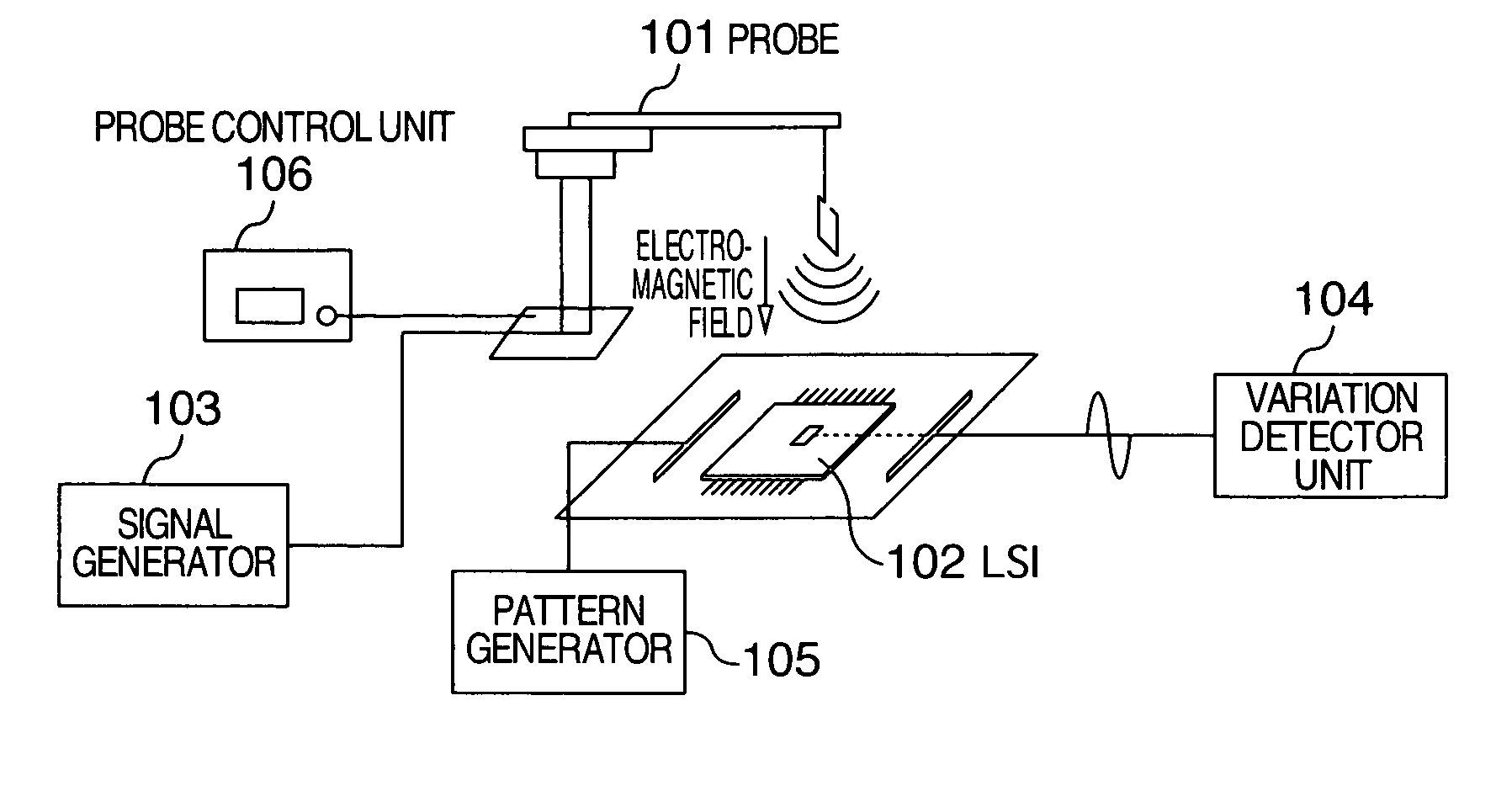
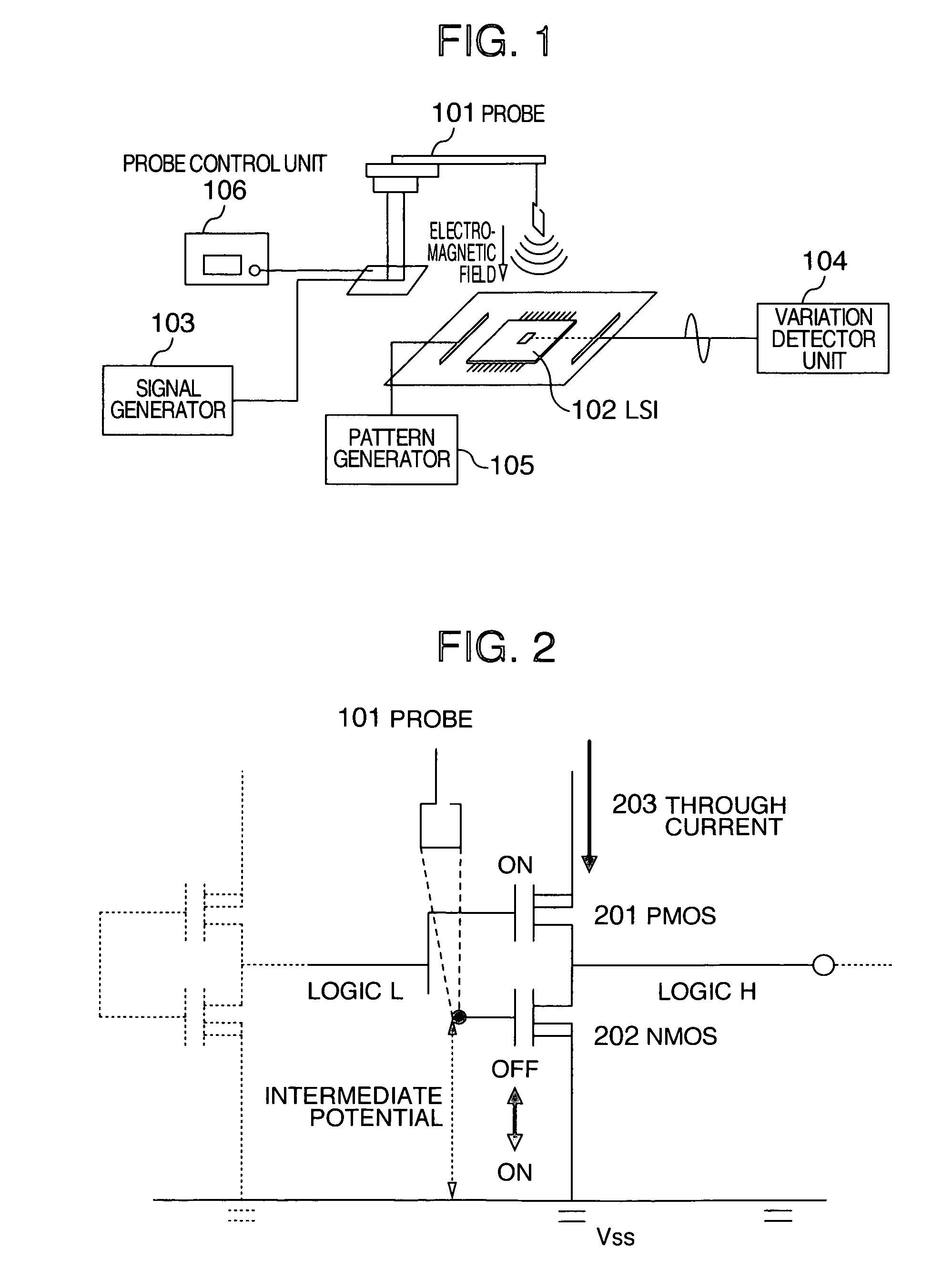
[0034]FIG. 1 shows a defect analysis apparatus for semiconductor integrated circuits according to the present invention. The defect analysis apparatus of the embodiment comprises a probe 101, an LSI 102, a signal generator 103, a variation detector unit 104, a pattern generator unit 105 for setting an LSI to a desired state, and a probe control unit 106.

[0035] The semiconductor defect analysis apparatus of the embodiment: (a) changes an intermediate potential of an open gate by applying an electric field, a magnetic field or the like emitted from the probe 101; (b) activates a gate circuit or a gate potential to generate a through current 203; (c) varies a power supply current of the circuit; and (d) measures this power supply current variation with the variation detector unit 104 to thereby identify a presence / absence of a defect.

[0036] For example, the probe 101 is first excited by a power supplied from the signal generator unit 103 to make the probe 101 generate an electric or m...

second embodiment

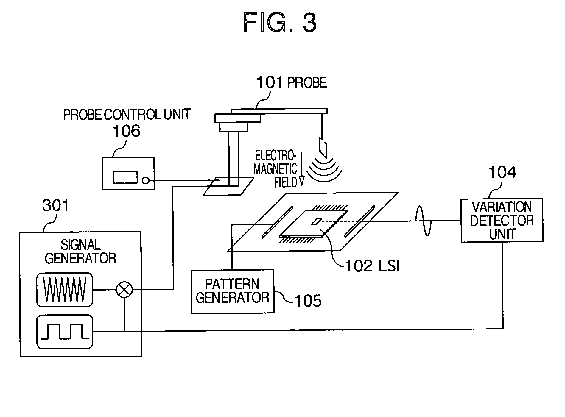
[0049] Next, with reference to FIG. 3, description will be made on a defect analysis apparatus, considering an operation of by-pass capacitors according to a

[0050] By-pass capacitors are added to an inside of a power supply system of LSI 102 or a test substrate mounted with LSI. With high frequency electric or magnetic field excitation, a power supply current variation caused by activation of a gate circuit occurs at a high frequency. Therefore, the variation is suppressed by the by-pass capacitors and is difficult to be detected with the variation detector unit 104. The defect analysis apparatus of this embodiment mitigates this problem.

[0051] The defect analysis apparatus of this embodiment comprises an electric or magnetic field probe 101, a variation detector unit 104, a pattern generator unit 105 for setting LSI to a desired state, a probe control unit 106, a signal generator 301 for modulating an excitation wave for supplying a power to the probe 101.

[0052] The signal genera...

third embodiment

[0057]FIG. 5 is a schematic view showing a defect analysis apparatus according to a The detect analysis apparatus of this embodiment comprises a probe 101, an LSI 102, a signal generator 103, a pattern generator unit 105 for setting LSI to a desired state, a probe control unit 106, a heat radiation and light emission analysis apparatus 501 and a detector unit 502. An electric or magnetic field is irradiated from the probe 101 to vary the potential of an open gate, activate the gate circuit and vary a power supply current.

[0058] In contrast with the above-described embodiment in which a power supply current variation is measured electrically directly, in the third embodiment a presence / absence of a defect portion is detected by capturing a physical phenomenon of heat radiation and light emission radiation from a gate circuit or its nearby area to be caused when an open gate or a gate potential is activated.


PUM


Abstract

The present invention aims at performing a semiconductor integrated circuit defect analysis with a simplified analysis apparatus and simplifying a defect analysis work. A defect analysis apparatus for a semiconductor integrated circuit is characterized in that a presence / absence of a defect is detected by irradiating an electromagnetic field from a probe to the semiconductor integrated circuit and detecting an electric characteristic variation such as a power supply current variation in the semiconductor integrated circuit.

Description

TECHNICAL FIELD [0001] The present invention relates to a semiconductor defect analysis apparatus and system and a semiconductor defect analysis method for supporting semiconductor defect analysis, and also relates to a semiconductor manufacture method. BACKGROUND ART [0002] Shortening a defect analysis time in the manufacture processes for semiconductor integrated circuits (hereinafter called LSI) is a very important issue from the standpoint of shortening a process configuration period and starting up quickly a process line. A delay in defect analysis leads to a delay in process configuration. [0003] However, recent LSIs with advanced miniaturization and high integration have an immense number of wiring patterns, resulting in a long analysis time. There occur the cases that a defect position cannot be identified and the analysis of LSI defects such as disconnection defect becomes difficult. [0004] As a conventional example of defect analysis techniques for detecting LSI wiring bre...

Claims


Application Information

Patent Timeline
Patent Type & Authority Applications(United States)
IPC IPC(8): G01R31/26G01R31/302G01R31/311H01L21/66
CPCG01R31/311
Inventor KOMIYA, YASUMAROKIKUCHI, SHUJIUESAKA, KOICHITOBA, TADANOBUYAMAMOTO, KEIICHI
Owner HITACHI LTD
Why Eureka
Try Eureka