Source driver and source driving method

a source driver and driver technology, applied in the direction of static indicating devices, amplifiers with semiconductor devices/discharge tubes, instruments, etc., can solve the problems of difficult pull-low differential amplifiers, and achieve the effect of reducing the number of differential amplifiers used for driving data lines, reducing the circuit size and the manufacturing cost of a source driving circui

Inactive Publication Date: 2006-07-27
HIMAX TECH LTD
View PDF3 Cites 14 Cited by
  • Summary
  • Abstract
  • Description
  • Claims
  • Application Information

AI Technical Summary

Benefits of technology

[0012] It is an object of the present invention to provide a source driver for LCDs, which can increase the driving voltage range and decrease the power consumption.
[0013] It is another object of the present invention to provide a source driver for LCDs, which can reduce the circuit size and the manufacturing cost of a source driving circuit.
[0015] The source driver according to the present invention further comprises a first switching circuit and a second switching circuit respectively used for alternatively switching a plurality of predetermined voltages and alternatively switching a plurality of output voltage of a plurality of data lines to the first and second differential amplifiers during a scanning line period, such that the plurality of output voltages at the plurality of data lines can be respectively driven through the first and second differential amplifiers according to the plurality of predetermined voltages. More specifically, since the plurality of data lines can share the first and second differential amplifiers, the circuit size and the manufacturing cost of a source driving circuit can be reduced.
[0017] According to the source driving method of the present invention, the two differential amplifiers can drive multiple data lines; therefore, the number of differential amplifiers used for driving data lines can be decreased whereby reducing the circuit size and the manufacturing cost of a source driving circuit.

Problems solved by technology

However, when the voltage level of the output voltage Vout is close to the voltage level of a high supply voltage VDD and smaller than that of the level voltage Vin, it is difficult for the pull-high differential amplifier 210 to pull up the output voltage Vout.
In addition, when the voltage level of the output voltage Vout is close to the voltage level of a low supply voltage VSS and larger than that of the level voltage Vin, it is difficult for the pull-low differential amplifier 212 to pull down the output voltage Vout.

Method used


Image

  • Source driver and source driving method
  • Source driver and source driving method
  • Source driver and source driving method

Examples


Embodiment Construction

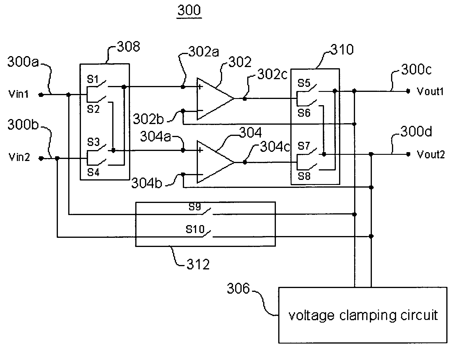
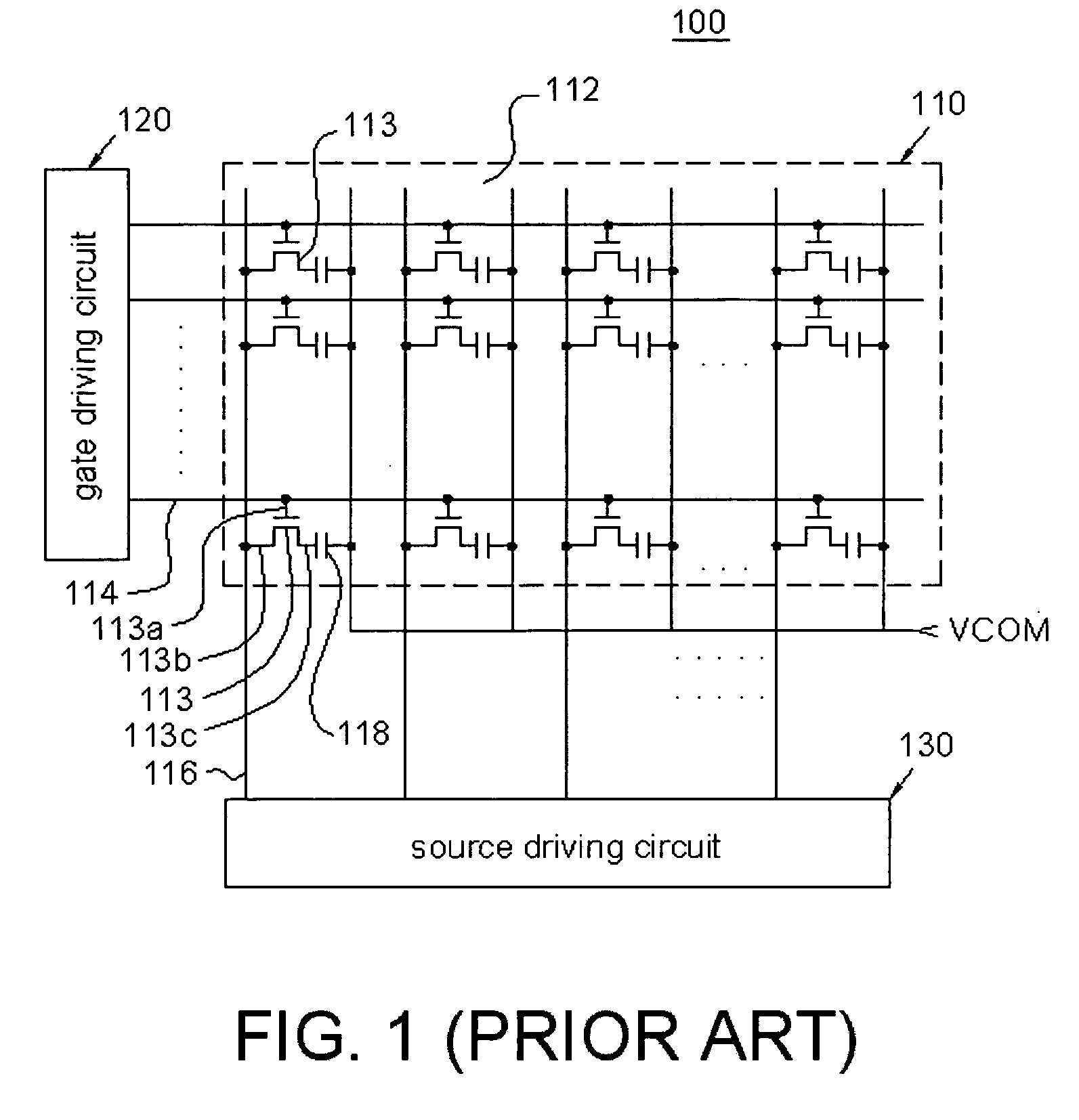
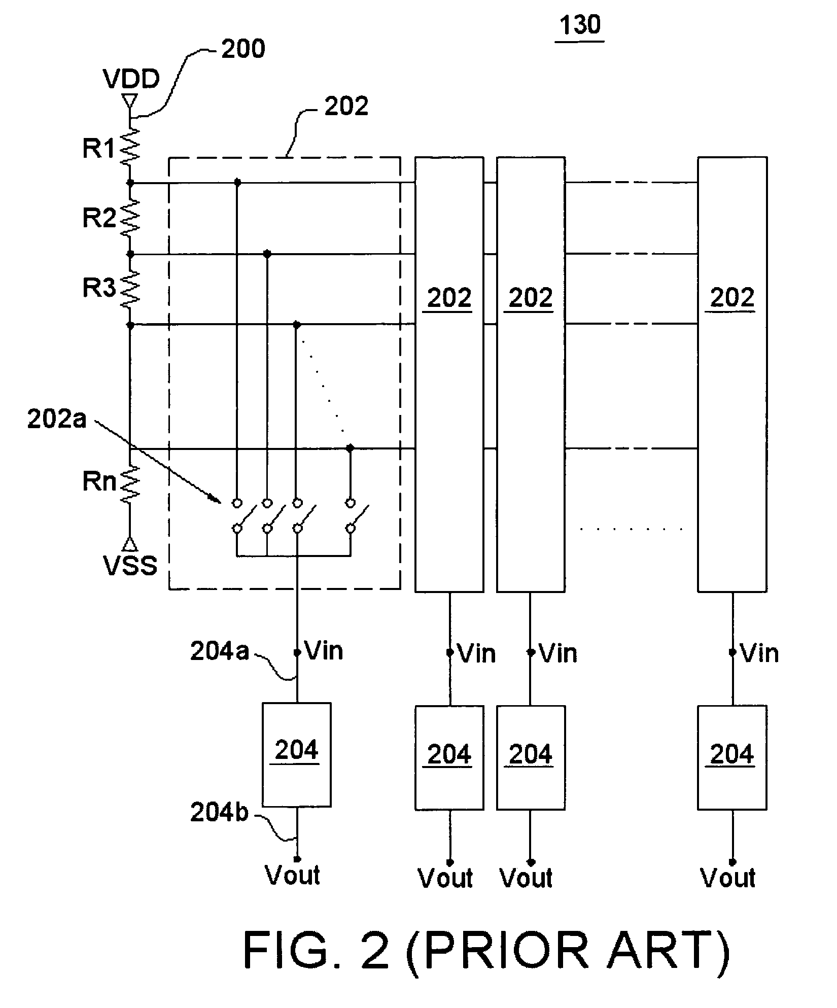
[0027]FIG. 4 is a circuit diagram of a source driver 300 for LCDs according to one embodiment of the present invention. The source driver 300 has two inputs 300a and 300b for respectively receiving level voltages Vin1 and Vin2 from a voltage divider (e.g. the voltage divider 200 shown in FIG. 2), and two outputs 300c and 300d for respectively and electrically being connected to two data lines disposed on an LCD panel (e.g. the data lines 116 shown in FIG. 1), wherein the outputs 300c and 300d respectively have output voltages Vout1 and Vout2. The source driver 300 includes a pull-high differential amplifier 302, a pull-low differential amplifier 304, a voltage clamping circuit 306, a first switching circuit 308, a second switching circuit 310 and a third switching circuit 312. The first switching circuit 308 has switches S1, S2, S3 and S4; the second switching circuit 310 has switches S5, S6, S7 and S8; and the third switching circuit 312 has switches S9 and S10.

[0028] The source d...


PUM


Abstract

A source driver for LCD devices, used for driving at least one data line, comprises an input for receiving a predetermined voltage; an output electrically being connected to the data line and having an output voltage; a voltage clamping circuit for clamping the output voltage within a predetermined voltage range; a first differential amplifier for increasing the clamped output voltage toward the predetermined voltage; and a second differential amplifier for decreasing the clamped output voltage toward the predetermined voltage. The present invention also provides a source driving method for LCD devices.

Description

CROSS REFERENCE TO RELATED APPLICATION [0001] This application claims the priority benefit of Taiwan Patent Application Serial Number 094102051, filed on Jan. 24, 2005, the full disclosure of which is incorporated herein by reference. BACKGROUND OF THE INVENTION [0002] 1. Field of the Invention [0003] This invention generally relates to a source driver and a source driving method, and more particularly to a source driver and source driving method for LCDs. [0004] 2. Description of the Related Art [0005]FIG. 1 is a conventional driving circuit for an active matrix LCD (liquid crystal display) device 100. The LCD device 100 includes an LCD panel 110 having a TFT (thin film transistor) array 112 disposed thereon, a gate driving circuit 120 and a source driving circuit 130. The TFT array 112 is formed by a plurality of thin film transistors 113. Each transistor 113 has its gate 113a connected to a corresponding scanning line 114, its source 113b connected to a corresponding data line 11...

Claims


Application Information

Patent Timeline
Patent Type & Authority Applications(United States)
IPC IPC(8): G09G3/36
CPCG09G3/3648G09G3/3688G09G3/3696G09G2320/0252G09G3/20G09G3/36
Inventor CHANG, YAW GUANGCHIU, MING CHENG
Owner HIMAX TECH LTD
Why Eureka
Try Eureka