Multi-transistor memory cells
a memory cell and multi-transistor technology, applied in the field of memory cells, can solve the problems achieve the effects of low power consumption, small area layout, and simple structur
- Summary
- Abstract
- Description
- Claims
- Application Information
AI Technical Summary
Benefits of technology
Problems solved by technology
Method used
Image

Examples
Embodiment Construction
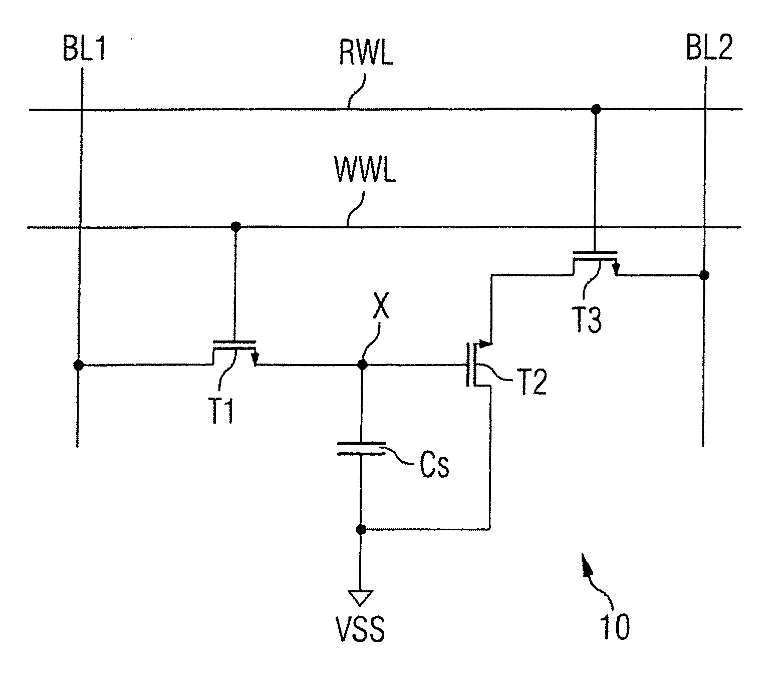
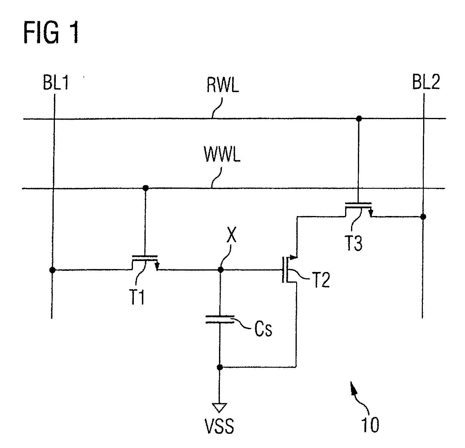
[0036]FIG. 1 shows a circuit diagram of a memory cell 10 having three transistors T1 to T3 and a capacitor Cs. In the exemplary embodiment, the transistors T1 to T3 are n-channel transistors. The capacitor Cs may be a metal insulator metal (“MIM”) capacitor. The circuit of the memory cell 10 includes a subcircuit for writing and a subcircuit for reading. The charge of the capacitor Cs is not altered during reading, so that there is no need either for the charge to be refreshed after a reading operation.
[0037] The subcircuit for writing includes the writing transistor T1 and the capacitor Cs. A gate of the transistor T1 is connected to a writing word line WWL. A drain of the transistor T1 is connected to a writing bit line BL1. The source connection of the transistor T1 leads to a memory node X formed by an electrode of the capacitor Cs. The other electrode of the capacitor Cs is at a ground potential VSS.
[0038] The subcircuit for reading includes transistors T2 and T3. A gate of t...
PUM
 Abstract
Description
Claims
Application Information