
Photoresist composition and method of forming a pattern using the same

Inactive Publication Date: 2006-07-27
SAMSUNG ELECTRONICS CO LTD
View PDF4 Cites 0 Cited by
  • Summary
  • Abstract
  • Description
  • Claims
  • Application Information

AI Technical Summary

Benefits of technology

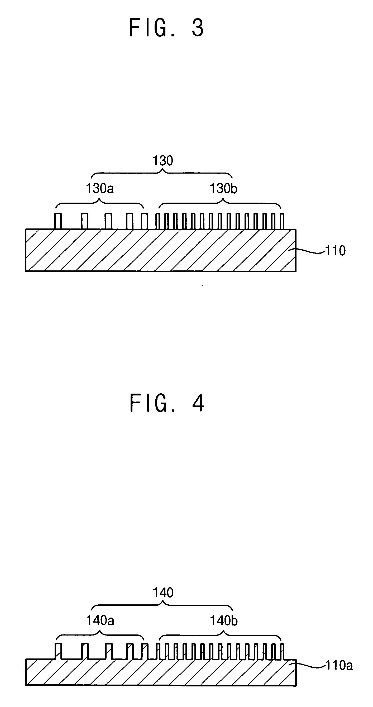
[0018] According to the present invention, the photoresist composition including a mixture of blocking groups is less sensitive to a temperature of the PEB process and an intensity change of the light irradiated to the photoresist composition, so that a solubility of the photoresist film in the iso-pattern region is sufficiently reduced. Accordingly, a line width of the iso-pattern reaches the target line width thereof, so the difference between the practical line width and the target line width of the iso-pattern is remarkably reduced

Problems solved by technology

In particular, difficulties are encountered when an ArF excimer laser is used as a light source of an exposure system and the baking process is performed at a temperature above 130° C. to form a photoresist pattern having a line width of no more than about 85 nm at a cell region, because the line width of the photoresist pattern at a peripheral region is very small compared to the target line width of the photoresist pattern at the peripheral region.
However, a photoresist composition with a high activation energy is undesirable for forming a photoresist pattern with a high resolution and a small critical dimension because the line width of the photoresist pattern formed with this type of photoresist composition will still be small at the peripheral portion of a substrate despite improving the processing margin of the EL.
Thus, when a subsequent etching process is performed using the photoresist pattern of which a line width deviates from the target line width as an etching mask, a lifting defect, in which a pattern is lifted from an underlying layer or a substrate, or a bridge defect in which neighboring patterns are interconnected with each other, may be formed when manufacturing a semiconductor device.

Method used


Image

  • Photoresist composition and method of forming a pattern using the same
  • Photoresist composition and method of forming a pattern using the same
  • Photoresist composition and method of forming a pattern using the same

Examples


example

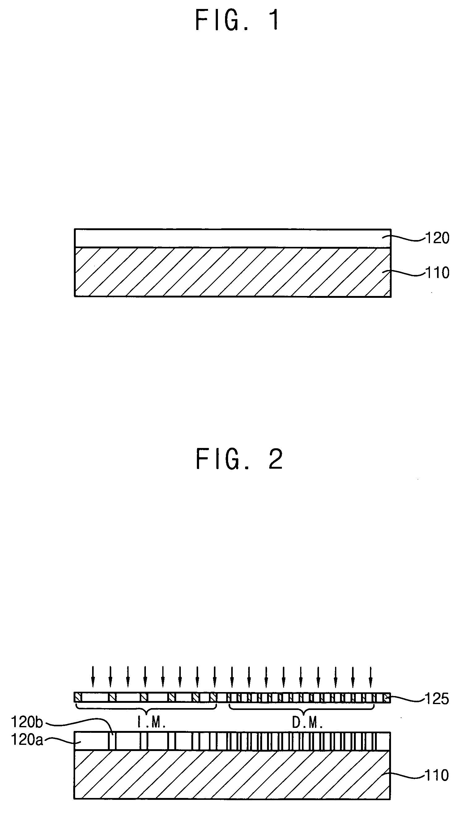
[0074] About 42 parts by weight of methyl acrylate including methyl adamantane, about 28 parts by weight of methacrylate including ethyl cyclohexane, about 25 parts by weight of monophenyl sulfonate, about 10 parts by weight of a quencher and about 895 parts by weight of a solvent were mixed with each other. The impurities were filtered off from the mixture by a 0.2 μm membrane filter, to thereby prepare a photoresist composition in accordance with an exemplary embodiment of the present invention that is then photo-chemically reacted with an ArF excimer laser. In this Example of the photoresist composition, the methyl acrylate was used as the first blocking group and the methacrylate was used as the second blocking group. Further, the monophenyl sulfonate was used as the PAG.


PUM


Abstract

A photoresist composition is provided. The photosensitive composition includes a photosensitive resin present in an amount of about 4% by weight to about 10% by weight, a photo-acid generator (PAG) present in an amount of about 0.1% by weight to about 0.5% by weight and a residual amount of a solvent. The photosensitive resin comprises a first resin which includes a first blocking group and a second resin which includes a second blocking group having an activation energy less than the first blocking group.

Description

CROSS-REFERENCES TO RELATED APPLICATIONS [0001] This application claims priority from Korean Patent Application No. 2005-6517 filed on Jan. 25, 2005, the content of which is incorporated by reference herein in its entirety. BACKGROUND OF THE INVENTION [0002] 1. Field of the Invention [0003] The present invention relates to a photoresist composition and a method of forming a pattern using the same. More particularly, the present invention relates to a photoresist composition of which a photosensitive resin comprises a mixture of blocking groups and a method of forming the photoresist pattern using the photoresist composition. [0004] 2. Description of the Related Art [0005] As semiconductor devices have become more highly integrated and are now operating at higher speeds, ultra-fine patterns having a line width of no more than about 100 nm are now needed. Conventionally, a photolithography process using a photosensitive material, such as a photoresist, is typically utilized in forming...

Claims


Application Information

Patent Timeline
IPC IPC(8): G03C1/76
CPCG03F7/0392G03F7/0045
Inventor KIM, KYOUNG-MIWANG, YOUN-KYUNGKIM, YOUNG-HO
Owner SAMSUNG ELECTRONICS CO LTD
Learn More